RT9264CS Просмотр технического описания (PDF) - Unspecified
Номер в каталоге
Компоненты Описание
Список матч
RT9264CS Datasheet PDF : 8 Pages
| |||
Preliminary
RT9264
Application Note
Output Voltage Setting
Referring to application circuits Fig.1 to Fig.3, the
output voltage of the switching regulator (VOUT1) can
be set with Eq.1.
The LDO output voltage can be set with Eq.2.
VOUT1 = (1+ RR21) ×1.25V
VOUT 2
=
(1+
R4
R3
)
×
0.86V
Eq.1
Eq.2
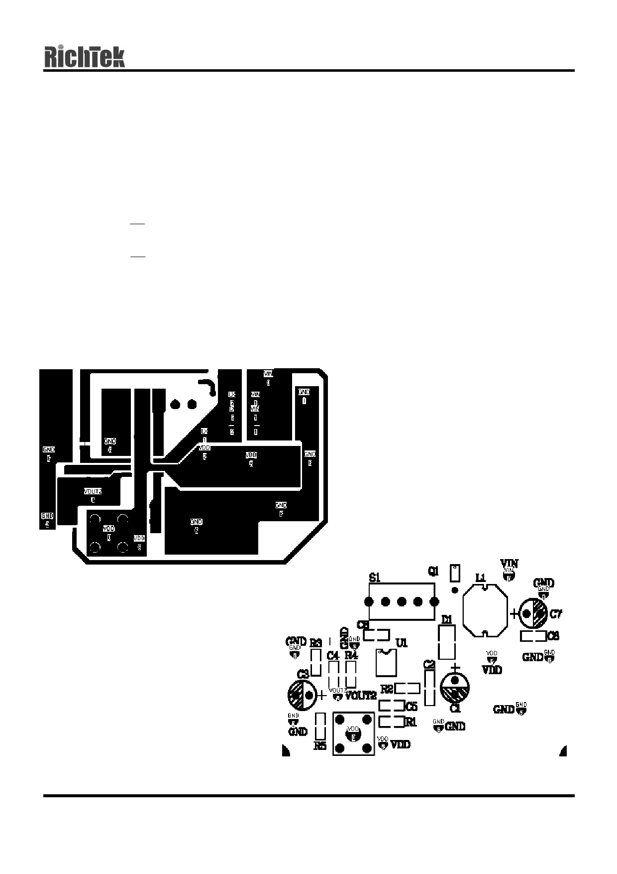
Layout Guide
• A full GND plane without gap break.
• VOUT1 to GND noise bypass – Short and wide
connection for C2 to Pin1 and Pin6.
• VIN to GND noise bypass – Add a 100µF capacitor
close to L1 inductor, when VIN is not an idea
voltage source.
• Minimized FB/LFB node copper area and keep far
away from noise sources.
• Minimized parasitic capacitance connecting to LX
and EXT nodes, which may cause additional
switching loss.
• The following diagram is an example of 2-layer
board layout for application circuits Fig.1 and
Fig.2.
First Layer
DS9264-00 December 2001
RT9264
Second Layer (Full GND Plane)
www.richtek-ic.com.tw
5
Share Link: 