V58C265404S-6 Просмотр технического описания (PDF) - Mosel Vitelic, Corp
Номер в каталоге
Компоненты Описание
Список матч
V58C265404S-6 Datasheet PDF : 44 Pages
| |||
MOSEL VITELIC
V58C265404S
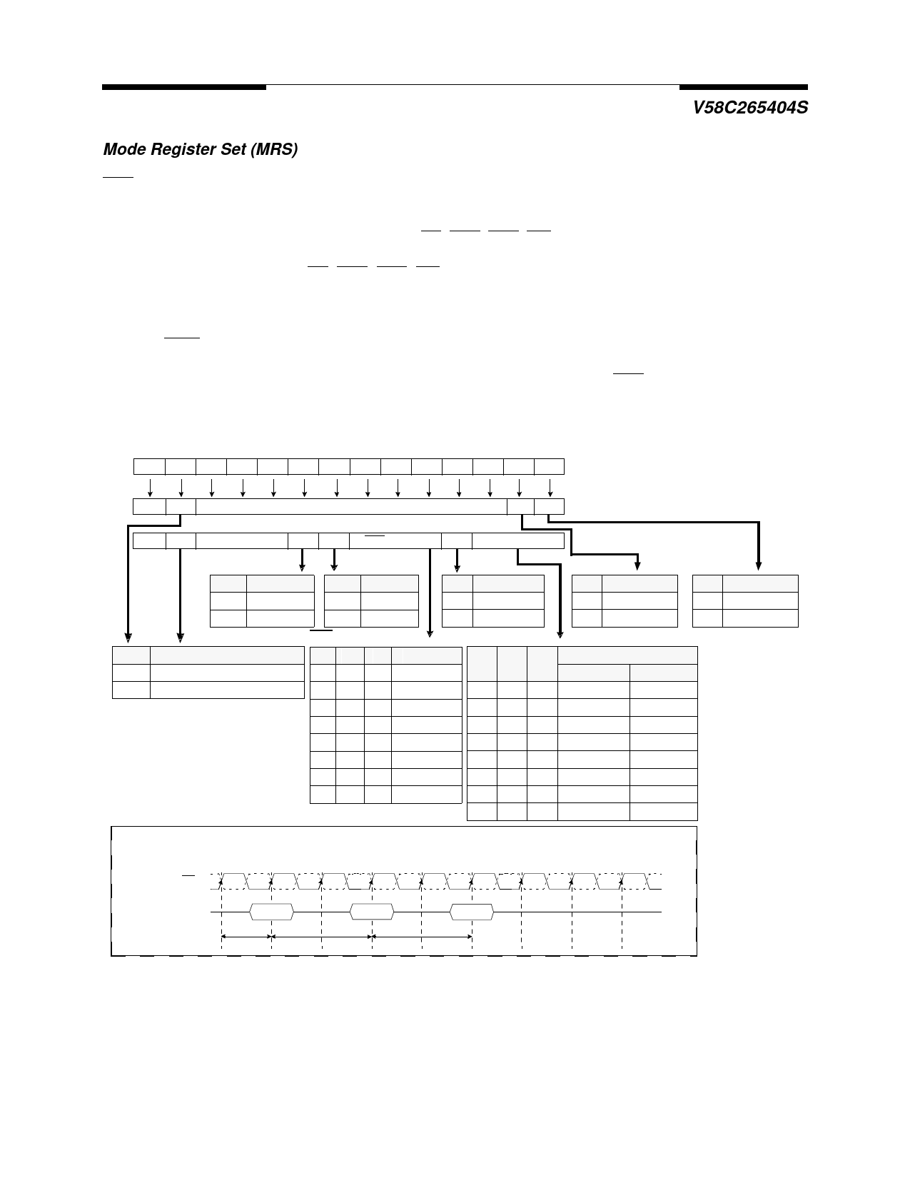
Mode Register Set (MRS)
The mode register stores the data for controlling the various operating modes of DDR SDRAM. It programs
CAS latency, addressing mode, burst length, test mode, DLL reset and various vendor specific options to
make DDR SDRAM useful for a variety of different applications. The default value of the mode register is not
defined, therefore the mode register must be written after EMRS setting for proper DDR SDRAM operation.
The mode register is written by asserting low on CS, RAS, CAS, WE and BA0 (The DDR SDRAM should be
in all bank precharge with CKE already high prior to writing into the mode register). The state of address pins
A0 ~ A11 in the same cycle as CS, RAS, CAS, WE and BA0 low is written in the mode register. Two clock
cycles are required to meet tMRD spec. The mode register contents can be changed using the same com-
mand and clock cycle requirements during operation as long as all banks are in the idle state. The mode reg-
ister is divided into various fields depending on functionality. The burst length uses A0 ~ A2, addressing mode
uses A3, CAS latency (read latency from column address) uses A4 ~ A6. A7 is a Mosel Vitelic specific test
mode during production test. A8 is used for DLL reset. A7 must be set to low for normal MRS operation. Refer
to the table for specific codes for various burst length, addressing modes and CAS latencies.
1. MRS can be issued only at all banks precharge state.
2. Minimum tRP is required to issue MRS command.
BA1 BA 0 A11 A10 A9 A8 A7 A6 A5 A4 A3 A2 A1 A0 Address Bus
0 MRS
0 MRS
RFU
RFU : Must be set "0"
I/O DLL Extended Mode Register
DLL TM CAS Latency BT Burst Length Mode Register
A8 DLL Reset
A7
mode
0
No
0 Normal
1
Yes
1
Test
CAS Latency
A3 Burst Type
0 Sequential
1 Interleave
Burst Length
BA0
An ~ A0
0
(Existing)MRS Cycle
1
Extended Funtions(EMRS)
* RFU(Reserved for future use)
should stay "0" during MRS
cycle.
A6 A5
00
00
01
01
10
10
11
11
A4 Latency
0 Reserve
1 Reserve
0
2
1
3
0 Reserve
1 Reserve
0
2.5
1 Reserve
A2 A1 A0
000
001
010
011
100
101
110
111
A1 I/O Strength
A0
0
Full
0
1
Half
1
Latency
Sequential Interleave
Reserve
Reserve
2
2
4
4
8
8
Reserve
Reserve
Reserve
Reserve
Reserve
Reserve
Reserve
Reserve
DLL Enable
Enable
Disable
Mode Register Set
0
1
2
3
4
5
6
7
8
CK, CK
Command
Precharge
All Banks
tCK
tRP *2
*1
Mode
Register Set
tMRD
Any
Command
V58C265404S Rev. 1.4 January 2000
6
Share Link: 