V58C265404SLT6 Просмотр технического описания (PDF) - Mosel Vitelic, Corp
Номер в каталоге
Компоненты Описание
Список матч
V58C265404SLT6 Datasheet PDF : 44 Pages
| |||
MOSEL VITELIC
V58C265404S
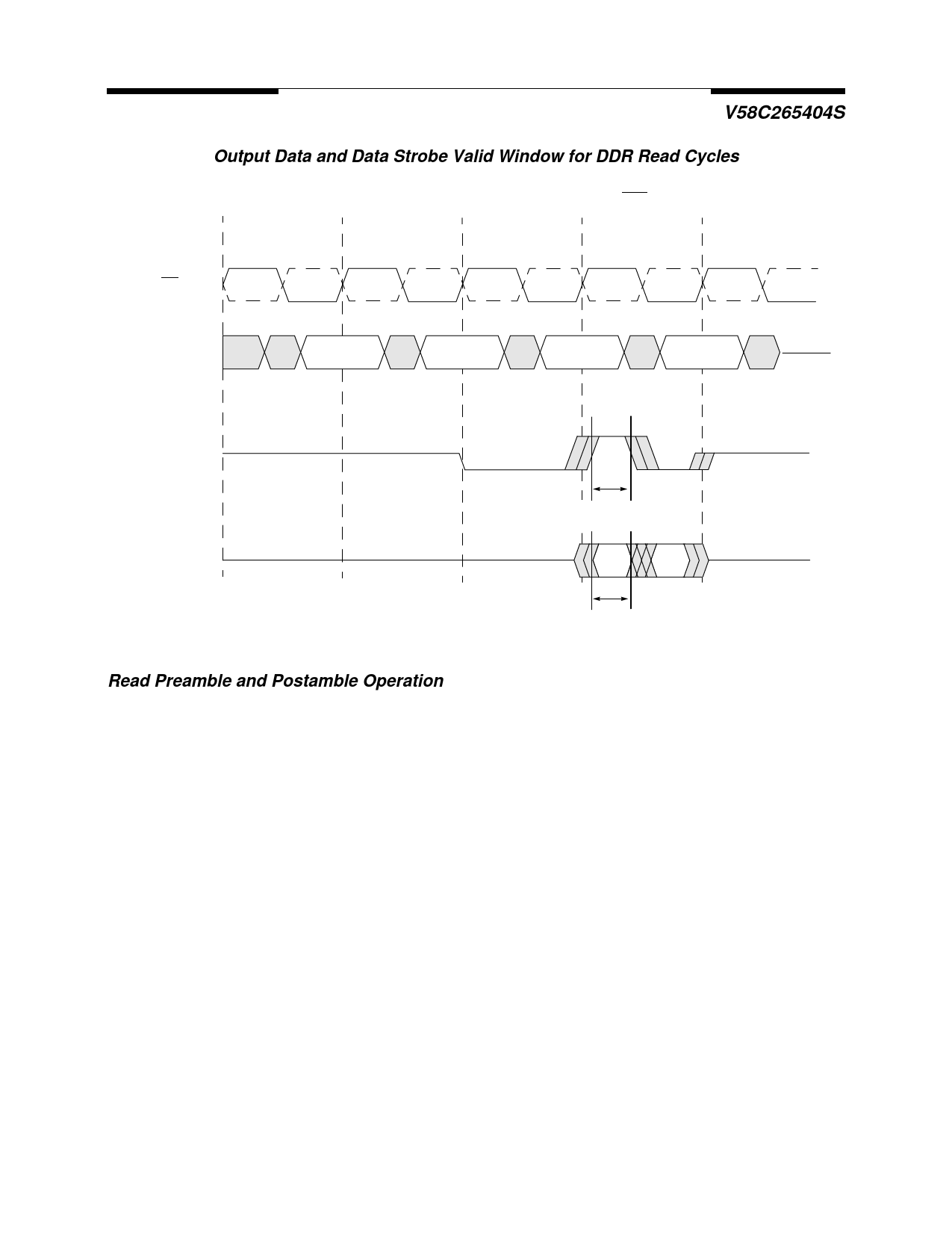
Output Data and Data Strobe Valid Window for DDR Read Cycles
(CAS Latency = 2; Burst Length = 2)
T0
T1
T2
T3
T4
CK, CK
Command
READ
NOP
NOP
NOP
DQS
DQ
tDQSV(min)
D0
D1
tDV(min)
Read Preamble and Postamble Operation
Prior to a burst of read data and given that the controller is not currently in burst read mode, the data strobe
signal (DQS), must transition from Hi-Z to a valid logic low. The is referred to as the data strobe “read pre-
amble” (tRPRE). This transition from Hi-Z to logic low nominally happens one clock cycle prior to the first edge
of valid data.
Once the burst of read data is concluded and given that no subsequent burst read operations are initiated,
the data strobe signal (DQS) transitions from a logic low level back to Hi-Z. This is referred to as the data
strobe “read postamble” (tRPST). This transition happens nominally one-half clock period after the last edge of
valid data.
Consecutive or “gapless” burst read operations are possible from the same DDR SDRAM device with no
requirement for a data strobe “read” preamble or postamble in between the groups of burst data. The data
strobe read preamble is required before the DDR device drives the first output data off chip. Similarly, the
data strobe postamble is initiated when the device stops driving DQ data at the termination of read burst cycles.
V58C265404S Rev. 1.4 January 2000
10
Share Link: 