V58C265804SLT7 Просмотр технического описания (PDF) - Mosel Vitelic, Corp
Номер в каталоге
Компоненты Описание
Список матч
V58C265804SLT7 Datasheet PDF : 44 Pages
| |||
MOSEL VITELIC
V58C265804S
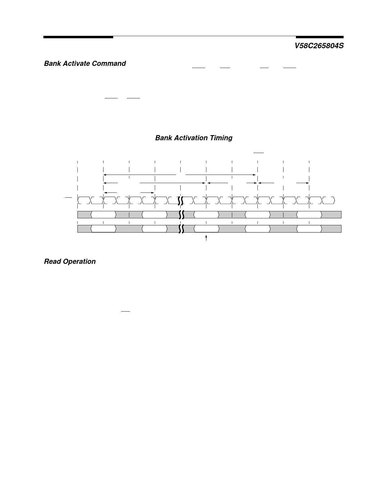
Bank Activate Command
The Bank Activate command is issued by holding CAS and WE high with CS and RAS low at the rising
edge of the clock. The DDR SDRAM has four independent banks, so two Bank Select addresses (BA0 and
BA1) are supported. The Bank Activate command must be applied before any Read or Write operation can
be executed. The delay from the Bank Activate command to the first Read or Write command must meet or
exceed the minimum RAS to CAS delay time (tRCD min). Once a bank has been activated, it must be pre-
charged before another Bank Activate command can be applied to the same bank. The minimum time interval
between interleaved Bank Activate commands (Bank A to Bank B and vice versa) is the Bank to Bank delay
time (tRRD min).
Bank Activation Timing
T0
T1
T2
T3
CK, CK
BA/Address
tRAS(min)
tRCD(min)
Bank/Row
Bank/Col
Command
Activate/A
Read/A
Tn
tRC
Tn+1
(CAS Latency = 2; Burst Length = Any)
Tn+2
Tn+3
Tn+4
Tn+5
tRP(min)
tRRD(min)
Bank
Pre/A
Bank/Row
Activate/A
Bank/Row
Activate/B
Begin Precharge Bank A
Read Operation
With the DLL enabled, all devices operating at the same frequency within a system are ensured to have
the same timing relationship between DQ and DQS relative to the CK input regardless of device density, pro-
cess variation, or technology generation.
The data strobe signal (DQS) is driven off chip simultaneously with the output data (DQ) during each read
cycle. The same internal clock phase is used to drive both the output data and data strobe signal off chip to
minimize skew between data strobe and output data. This internal clock phase is nominally aligned to the
input differential clock (CK, CK) by the on-chip DLL. Therefore, when the DLL is enabled and the clock fre-
quency is within the specified range for proper DLL operation, the data strobe (DQS), output data (DQ), and
the system clock (CK) are all nominally aligned.
Since the data strobe and output data are tightly coupled in the system, the data strobe signal may be de-
layed and used to latch the output data into the receiving device. The tolerance for skew between DQS and
DQ (tDQSQ) is tighter than that possible for CK to DQ (tAC) or DQS to CK (tDQSCK).
V58C265804S Rev. 1.3 January 2000
8
Share Link: 