3554 Просмотр технического описания (PDF) - Anaren Microwave
Номер в каталоге
Компоненты Описание
Список матч
3554 Datasheet PDF : 6 Pages
| |||
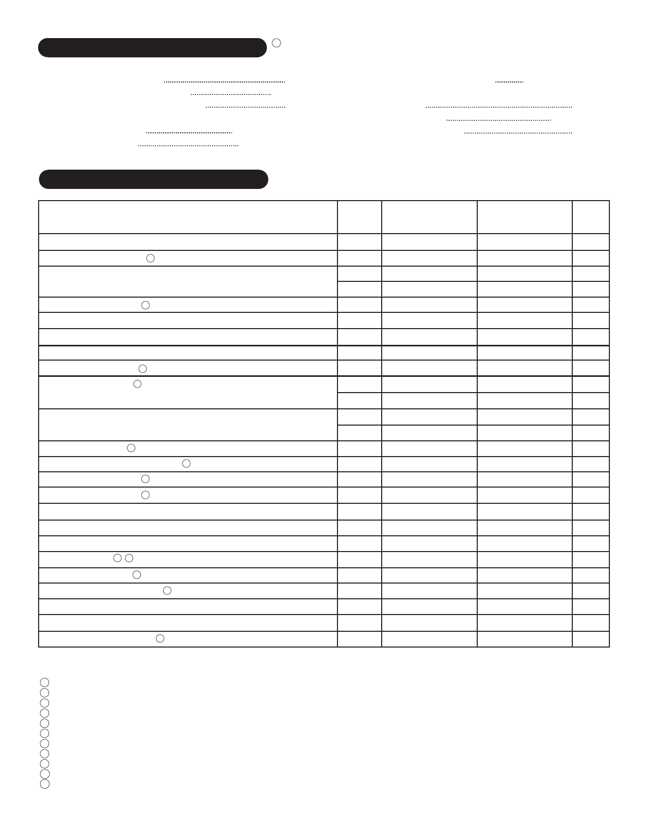
ABSOLUTE MAXIMUM RATINGS 11
±VCC
IOUT
VIN
TC
Supply Voltage
±18V
Peak Output Current
±150mA
Differential Input Voltage
±25V
Case Operating Temperature
MSK3554B
-55°C to +125°C
MSK3554
-40°C to +85°C
TST Storage Temperature Range
TLD Lead Temperature Range
(10 Seconds)
PD Power Dissipation
TJ Junction Temperature
-65°C to +150°C
300°C
See Curve
175°C
ELECTRICAL SPECIFICATIONS
Parameter
STATIC
Supply Voltage Range 3
Quiescent Current
Thermal Resistance 3
INPUT
Input Offset Voltage
Input Offset Voltage Drift
Input Offset Adjust 3
Input Bias Current 10
Input Offset Current
Input Impedance 3
Power Supply Rejection Ratio
Input Noise Density 3
Input Noise Voltage 3
OUTPUT
Output Voltage Swing
Output Current
Settling Time 2 3
Power Bandwidth 3
Bandwidth (Small Signal) 3
TRANSFER CHARACTERISTICS
Slew Rate
Open Loop Voltage Gain 3
Test Conditions
Group A
MSK3554B
MSK3554
Subgroup Min. Typ. Max. Min. Typ. Max.
VIN=0V
AV=-1V/V
Junction to Case Output Devices
-
±12 ±15 ±18 ±12 ±15 ±18
1
-
±14 ±20 -
±14 ±20
2,3
-
-
±30 -
-
-
-
-
37
-
-
37
-
Bal.Pins=N/C VIN=0V AV=-10V/V
VIN=0V
RPOT=20KΩ To +VCC AV=-1V/V
VCM=0V Either Input
VCM=0V
F=DC Differential
3
∆ VCC=10V
F=1KHz
F=10Hz To 1MHz
1
2,3
1,2,3
1
2,3
1
2,3
-
-
-
-
-
±0.5 ±2.0
-
±20 ±50
Adjust to Zero
-
±10 ±50
-
±10 ±50
-
±2.0 ±25
-
±2.0 ±30
-
10 11
-
80
110
-
-
15
-
-
10.0
-
-
±0.5 ±3.0
-
±20
-
Adjust to Zero
-
±20 ±100
-
-
-
-
±2.0 ±30
-
-
-
-
10 11
-
80
110
-
-
15
-
-
10.0
-
RL=100Ω
TJ<150°C
0.1% 10V step
RL=100Ω VO=±10V CC=0
CC=0
4
±10.5 ±12
- ±10 ±12
-
4
±100 ±120
- ±100 ±120
-
4
-
120 150 -
120 150
4
16
19
-
15
19
-
4
70
90
-
70
90
-
VOUT=±10V RL=100Ω CC=0
4
800 1200
- 750 1200
-
CC=0 RL=100Ω F=1KHz VOUT=±10V
4
90
96
-
88
96
-
Units
V
mA
mA
°C/W
mV
µV/°C
mV
pA
nA
pA
nA
Ω
dB
nV√Hz
µVrms
V
mA
nS
MHz
MHz
V/µS
dB
NOTES:
1 Unless otherwise specified ±VCC=±15VDC
2 AV=-1, measured in false summing junction circuit.
3 Devices shall be capable of meeting the parameter, but need not be tested. Typical parameters are for reference only.
4 Industrial grade devices shall be tested to subgroups 1 and 4 unless otherwise specified.
5 Military grade devices ('B' suffix) shall be 100% tested to subgroups 1,2,3 and 4.
6 Subgroup 5 and 6 testing available upon request.
7 Subgroup 1,4
TA=TC=+25°C
8 Subgroup 2,5
TA=TC=+125°C
9 Subgroup 3,6
TA=TC=-55°C
10 Measurement taken .5 second after application of power using automatic test equipment.
11 Continuous operation at or above absolute maximum ratings may adversely effect the device performance and/or life cycle.
2
8548-155 Rev. E 10/15
Share Link: 