MB86613 Просмотр технического описания (PDF) - Fujitsu
Номер в каталоге
Компоненты Описание
Список матч
MB86613 Datasheet PDF : 36 Pages
| |||
MB86613
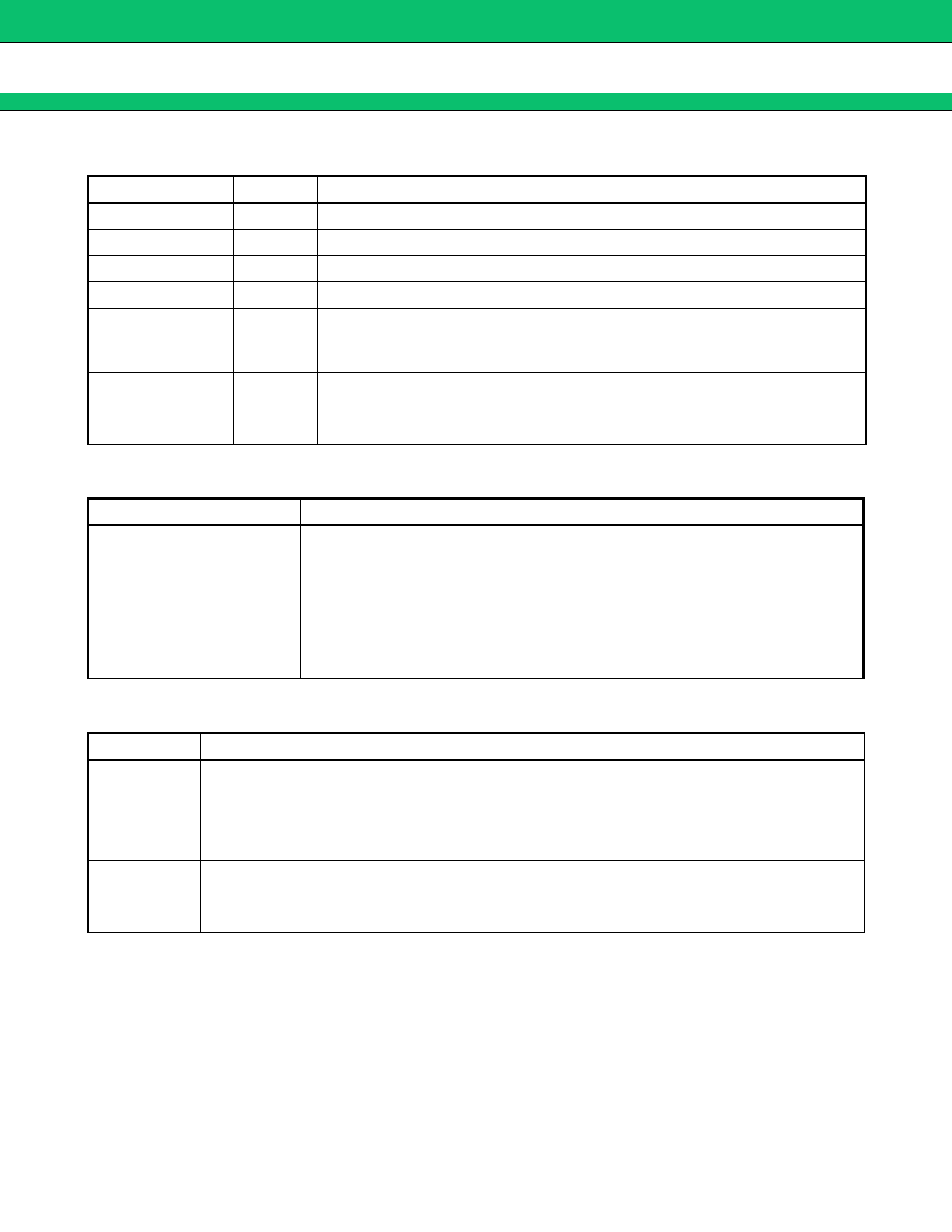
3. 1394 Interface Pin Description
Pin name
I/O
Function
TPA2 to TPA0
I/O Differential I/O positive terminal of 1394 bus port A
TPB2 to TPB0
I/O Differential I/O positive terminal of 1394 bus port B
TPA2# to TPA0#
I/O Differential I/O negative terminal of 1394 bus port A
TPB2# to TPB0#
I/O Differential I/O negative terminal of 1394 bus port B
TPBIAS2 to
TPBIAS0
1394 bus bias voltage supply pin.
O
For connecting a terminal resistor to TPBIAS and TPA/B, see “ sCOMPONENT
CONNECTION DIAGRAM 1. 1394 Ports”.
CPS
I
Cable power input pin
RO
O
Connect a 5.1 kΩ resistor between the RO and GND pins.
For details, see “ sCOMPONENT CONNECTION DIAGRAM 1. 1394 Ports”.
4. Internal PLL Pin Description
Pin name
I/O
Function
CLK
I
Internal PLL clock input pin.
Input a 24.576 MHz clock signal.
RF
O
Connect a 5.6 kΩ resistor between the RO and GND pins.
For details, see “ sCOMPONENT CONNECTION DIAGRAM 2. Filter Circuit”.
Filter circuit connection pin.
FIL
O
For connecting the filter circuit, see “ sCOMPONENT CONNECTION DIAGRAM
2. Filter Circuit”.
5. Miscellaneous Pin Description
Pin name
I/O
Function
CSCLK
This pin inputs the trigger signal for sending a cycle start packet during cycle master
operation.
I
Input an 8 kHz (125 µs) clock signal.
If the CLK pin is not used (with no Link Control. cycle Source bit set), however, con-
nect this pin to GND.
TEST
I
This pin in used for test mode.
During normal operation, leave this pin connected to GND.
N.C.
Leave this pin unconnected.
12
Share Link: 