GL6840 Просмотр технического описания (PDF) - Hynix Semiconductor
Номер в каталоге
Компоненты Описание
Список матч
GL6840 Datasheet PDF : 8 Pages
| |||
GL6840
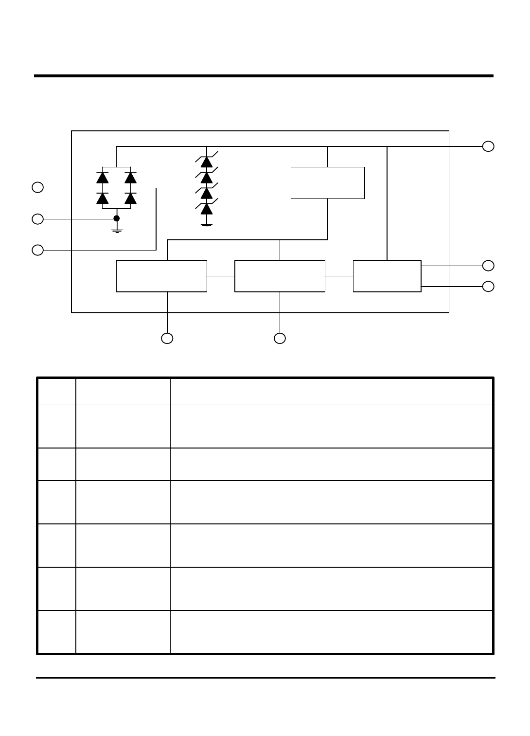
Block Diagram
7
Bridge
8
Diode
Threshold
Detector
Overvoltage
2
Protection
1
5
Sweep Frequency
Tone Generation
Output
Oscillator
Oscillator
Stage
6
3
4
Pin Description
PIN
NAME
DESCRIPTION
1,8
LINE
Input terminals to bridge diode. The AC ringing signal from the
telephone line drives the ringer through bridge.
2
GND
Ground
3
Sweep Rate This pin is connected to external capacitor to control the sweeping
Control Capacitor frequency(fSWEEP)
4
Output Frequency This pin is connected to external resistor to control the two tone
Control Resistor frequency(f1, f2)
5,6
Buzzer
The tone ringer output terminals which have inverse output phase
each others.
7
Rectifier
Capacitor
This pin is connected to external capacitor to change AC ringing
signal into DC voltage.
2
Share Link: 