RS5C372A Просмотр технического описания (PDF) - RICOH Co.,Ltd.
Номер в каталоге
Компоненты Описание
Список матч
RS5C372A Datasheet PDF : 59 Pages
| |||
RS5C372A/B
2. Registers
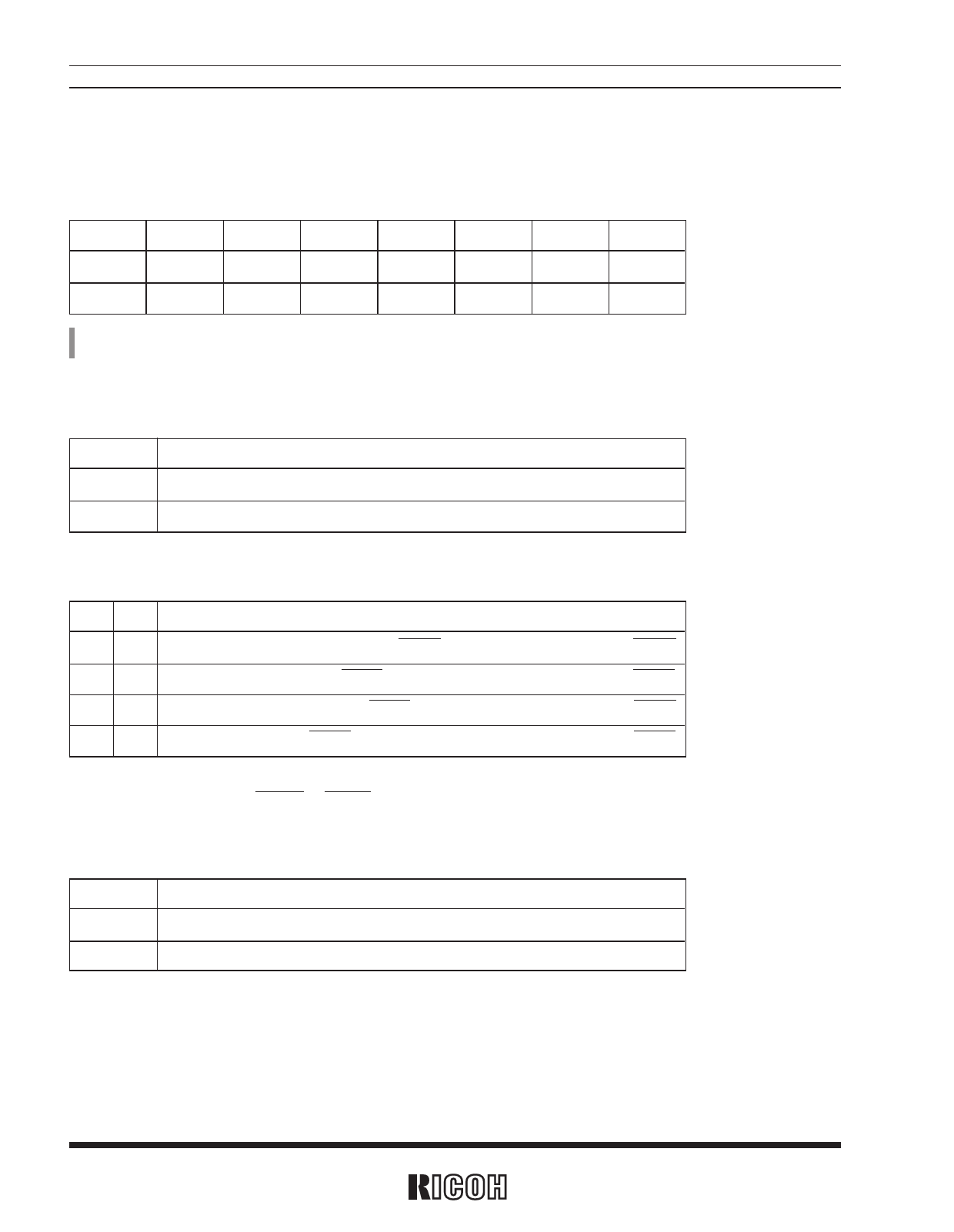
2.1 Control Register 1 (at internal address Eh)
D7
D6
D5
D4
D3
D2
D1
D0
AALE
BALE
SL2 *2
SL1 *2
TEST
CT2
CT1
CT0
AALE
BALE
SL2 *2
SL1 *2
TEST
CT2
CT1
CT0
0
0
0
0
0
0
0
0
*1) The default means read value when XSTP bit is set to “1” by starting up from 0V, or supply voltage drop, etc.
*2) SL1 and SL2 apply to the RS5C372A. For the RS5C372B, these bits must be filled with “0”.
2.1-1 AALE, BALE
Alarm_A, Alarm_B enable bits
AALE, BALE
Description
0
Alarm_A (Alarm_B) Correspondence action invalid
1
Alarm_A (Alarm_B) Correspondence action valid
(For write operation)
(For read operation)
Default*
(Default)
2.1-2 SL2, SL1 (RS5C372A only)
Interrupt output select bits
SL2 SL1
Description
0
0 Outputs Alarm_A, Alarm_B, INT to the INTRA. Outputs 32k clock pulses to the INTRB. (Default)
0
1 Outputs Alarm_A, INT to the INTRA. Outputs 32k clock pulses, Alarm_B to the INTRB.
1
0 Outputs Alarm_A, Alarm_B to the INTRA. Outputs 32k clock pulses, INT to the INTRB.
1
1 Outputs Alarm_A to the INTRA. Outputs 32k clock pulses, Alarm_B, INT to the INTRB.
By setting SL1 and SL2 bits, two alarm pulses (Alarm_A and alarm_B), periodic interrupt output (INT), 32k clock
pulses may be output to the INTRA or INTRB pins selectively.
2.1-3 TEST
Test bit
TEST
0
Ordinary operation mode
1
Test mode
Description
(Default)
The test bit is used for IC test. Set the TEST bit to 0 in ordinary operation.
16
Share Link: 