RS5C372B Просмотр технического описания (PDF) - RICOH Co.,Ltd.
Номер в каталоге
Компоненты Описание
Список матч
RS5C372B Datasheet PDF : 59 Pages
| |||
RS5C372A/B
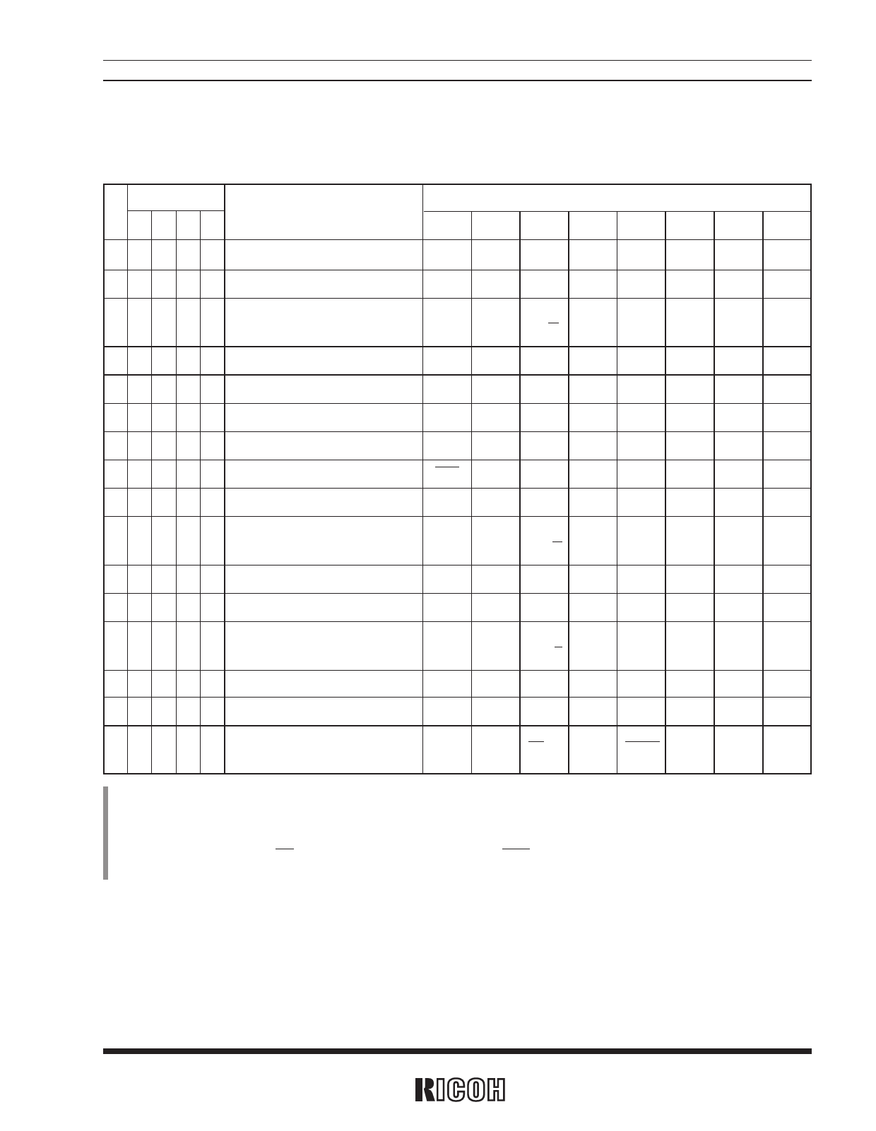
FUNCTIONAL DESCRIPTIONS
1. Allocation of Internal Addresses
Internal address
A3 A2 A1 A0
Contents
0 0 0 0 0 Second Counter
Data*1
D7
D6
D5
D4
D3
D2
D1
D0
—*2
S40
S20
S10
S8
S4
S2
S1
1 0 0 0 1 Minute Counter
—
M40 M20 M10
M8
M4
M2
M1
2 0 0 1 0 Hour Counter
H20
—
—
H10
H8
H4
H2
H1
P/A
3 0 0 1 1 Day of the Week Counter
—
—
—
—
—
W4
W2
W1
4 0 1 0 0 Day Counter
—
—
D20
D10
D8
D4
D2
D1
5 0 1 0 1 Month Counter
—
—
— MO10 MO8 MO4 MO2 MO1
6 0 1 1 0 Year Counter
Y80
Y40
Y20
Y10
Y8
Y4
Y2
Y1
7 0 1 1 1 Time Trimming Register
XSL F6
F5
F4
F3
F2
F1
F0
8 1 0 0 0 Alarm_A (Minute Register)
— AM40 AM20 AM10 AM8 AM4 AM2 AM1
9 1 0 0 1 Alarm_A (Hour Register)
AH20
—
—
AH10 AH8 AH4 AH2 AH1
AP/A
A 1 0 1 0 Alarm_A (Day of the Week Register) — AW6 AW5 AW4 AW3 AW2 AW1 AW0
B 1 0 1 1 Alarm_B (Minute Register)
— BM40 BM20 BM10 BM8 BM4 BM2 BM1
C 1 1 0 0 Alarm_B (Hour Register)
BH20
—
—
BH10 BH8 BH4 BH2 BH1
BP/A
D 1 1 0 1 Alarm_B (Day of the Week Register) — BW6 BW5 BW4 BW3 BW2 BW1 BW0
E 1 1 1 0 Control Register 1
AALE BALE SL2*5 SL1*5 TEST CT2 CT1 CT0
F 1 1 1 1 Control Register 2
ADJ *3
—
— 12/24 XSTP*4 CLEN CTFG AAFG BAFG
*1) All the listed data can be read and written except for ADJ/XSTP.
*2) The “–” mark indicates data which can be read only and set to “0” when read.
*3) The ADJ/XSTP bit of the control register2 is set to ADJ for write and XSTP for read operation. The XSTP bit is set to “0” by writing data into the con-
trol register2 for normal oscillation.
*4) When XSTP is set to “1”, the XSL, F6 to F0, CT2 to CT0, AALE, BALE, SL2, SL1, CLEN and TEST bits are reset to “0”.
*5) SL1 and SL2 apply to the RS5C372A. For the RS5C372B, these bits must be filled with “0”.
15
Share Link: 