HPMX-5002-TR1 Просмотр технического описания (PDF) - HP => Agilent Technologies
Номер в каталоге
Компоненты Описание
Список матч
HPMX-5002-TR1 Datasheet PDF : 14 Pages
| |||
IP1
OSCOP
OSCOPB
IFIP1
IF1
DMOD
IFOP1
DMODOP
BUF1
BUF2
TCSET
90/216
φ
FREQ.
DET.
RSSI
CHARGE
PUMP
LOCK
DET.
DATA
SLICER
9/12/16
BIAS
CONTROL
VCOADJ VCOB
PFD
VCOA
DIV3
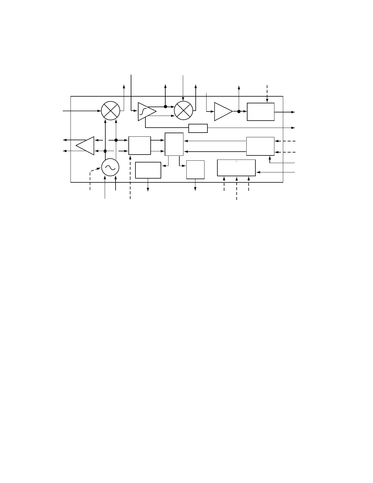
Figure 2. HPMX-5002 Detailed Block Diagram.
LKDET
PLL
XLO
RX
DATAOP
RSSI
DIV2
DIV1
REF
BGR
Functional Description
Please refer to Figure 2, Detailed
Block Diagram, above. Figure 2
contains a graphical representa-
tion of all 32 active signal pins of
the HPMX-5002. For clarity, the
supply, ground, and substrate pins
are deleted.
Modes of Operation
The HPMX-5002 supports four
basic modes of operation. The logic
states necessary to program each
mode are listed in Table 1, Mode
Programming. The modes are:
Receive mode (RX),
which is used during the receive
time slot in DECT systems. All
blocks are powered on in this
mode.
LO2 synthesis mode (PLL),
which enables the IC to achieve
phase lock without biasing the
receive signal path, thus saving
power. This is very useful for
DECT blind-slot applications.
Transmit mode (TX),
designed for use when the LO2
VCO is directly modulated by the
DECT data stream for subsequent
up-conversion to the channel
frequency (with the HPMX-5001
DECT Upconverter/Down-
converter). In this mode, only the
VCO and LO2 output buffer are
biased and operational. In order
to use the LO2 VCO as a modula-
tion source, it is necessary to first
program the HPMX-5002 in PLL
mode. Once the loop has achieved
lock, the PLL is then disabled by
setting the PLL pin to a logic 0.
This puts the VCO into “flywheel”
operation, preventing the PLL
from interfering with the modula-
tion of the VCO. Leakage in the
tank circuit shown in Figure 3
allows the VCO to drift at a rate of
2.5 kHz per mS, well within the
DECT specs of 13 kHz per mS.
Standby mode,
where all blocks are powered
down. This mode allows the
system designer to effectively turn
the IC off without having to use
battery control, and also allows
the IC to change quickly to an
active mode.
Detailed Circuit
Description
PLL Section
The PLL section of the
HPMX-5002 contains three major
sections: a set of reference and
LO2 dividers, a phase/frequency
detector with charge pump, and a
lock detector.
The dividers for both the refer-
ence and LO2 signals in the PLL
section are programmable to
accomodate the most popular
DECT reference frequencies and
also to enable the use of higher
1st IF frequencies if desired.
7-111
Share Link: 