HD74HC91RPEL Просмотр технического описания (PDF) - Renesas Electronics
Номер в каталоге
Компоненты Описание
Список матч
HD74HC91RPEL Datasheet PDF : 6 Pages
| |||
HD74HC91
8-bit Shift Register
REJ03D0696-0200
(Previous ADE-205-429)
Rev.2.00
Oct 06, 2005
Description
This serial-in, serial-out, 8-bit shift register is composed of eight R-S master-slave flip-flops, input gating, and a clock
drive. Single-rail data and input control are gated through inputs A and B and an internal inverter to form the
complementary inputs to the first bit of the shift register. Drive for the internal common clock line is provided by an
inverting clock driver. This clock pulse inverter/driver causes these circuits to shift information one bit on the positive
edge of an input clock pulse.
Features
• High Speed Operation: tpd (Data Word Input to Output) = 21 ns typ (CL = 50 pF)
• High Output Current: Fanout of 10 LSTTL Loads
• Wide Operating Voltage: VCC = 2 to 6 V
• Low Input Current: 1 µA max
• Low Quiescent Supply Current: ICC (static) = 4 µA max (Ta = 25°C)
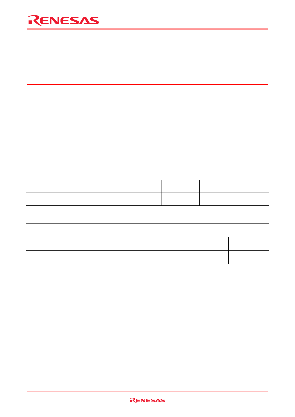
• Ordering Information
Part Name
Package Type
Package Code
(Previous Code)
Package
Abbreviation
HD74HC91RPEL
SOP-14 pin (JEDEC)
PRSP0014DE-A
(FP-14DNV)
RP
Taping Abbreviation
(Quantity)
EL (2,500 pcs/reel)
Function Table
Inputs
tn
A
B
H
H
L
X
X
L
H : High level
L : Low level
X : Irrelevant
tn : Reference bit time, clock low
tn + 8 : Bit time after 8 low-to-high clock transitions
Outputs
tn + 8
QH
QH
H
L
L
H
L
H
Rev.2.00, Oct 06, 2005 page 1 of 5
Share Link: 