CS8126 Просмотр технического описания (PDF) - Cherry semiconductor
Номер в каталоге
Компоненты Описание
Список матч
CS8126 Datasheet PDF : 9 Pages
| |||
Absolute Maximum Ratings
Power Dissipation.............................................................................................................................................Internally Limited
Peak Transient Voltage (46V Load Dump) .................................................................................................................-50V, 60V
Output Current .................................................................................................................................................Internally Limited
ESD Susceptibility (Human Body Model)..............................................................................................................................4kV
Junction Temperature .............................................................................................................................................-40¡C to 150¡C
Storage Temperature...............................................................................................................................................-55¡C to 150¡C
Lead Temperature Soldering Wave Solder (through hole styles only) ..........................................10 sec. max, 260¡C peak
Reflow (SMD styles only) ..........................................60 sec. max above 183¡C, 230¡C peak
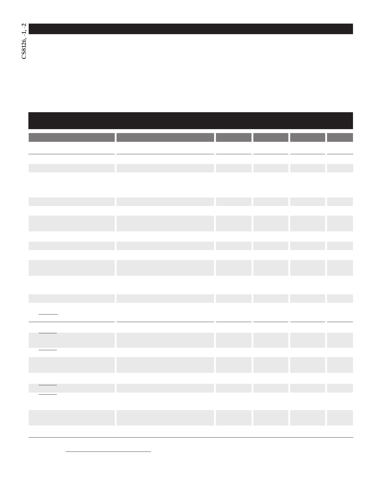
Electrical Characteristics: TA = -40ûC to +125ûC, TJ = -40ûC to +150ûC, VIN = 6 to 26V, IO=5 to 500mA,
RRESET = 4.7k½ to VCC, unless otherwise noted.
PARAMETER
s Output Stage (VOUT)
Output Voltage
Dropout Voltage
Supply Current
Line Regulation
Load Regulation
Ripple Rejection
Current Limit
Overvoltage Shutdown
Maximum Line Transient
Reverse Polarity Input
Voltage DC
Reverse Polarity Input
Voltage Transient
Thermal Shutdown
TEST CONDITIONS
IOUT = 500mA
IOUT ² 10mA
IOUT ² 100mA
IOUT ² 500mA
VIN = 6 to 26V, IOUT = 50mA
IOUT = 50 to 500mA, VIN = 14V
f = 120Hz, VIN = 7 to 17V,
IOUT = 250mA
VOUT ² 5.5V
VOUT ³ -0.6V, 10½ Load
1% Duty Cycle, T < 100ms,
10½ Load
Guaranteed by Design
MIN
4.85
54
0.75
32
-15
150
TYP
5.00
0.35
2
6
55
5
10
75
1.20
95
-30
-80
180
MAX
5.15
0.60
7
12
100
50
50
40
210
UNIT
V
V
mA
mV
mV
dB
A
V
V
V
V
¡C
s RESET and Delay Functions
Delay Charge Current
VDelay = 2V
5
RESET Threshold
VOUT Increasing, VRT(ON)
4.65
VOUT Decreasing, VRT(OFF)
4.50
RESET Hysteresis
VRH = VRT(ON) - VRT(OFF)
150
Delay Threshold
Charge, VDC(HI)
3.25
Discharge, VDC(LO)
2.85
Delay Hysteresis
200
RESET Output Voltage Low
RESET Output Leakage
Current
1V < VOUT < VRTL , 3k½ to VOUT
VOUT > VRT(ON)
Delay Capacitor
Discharge Latched ÒONÓ,
Discharge Voltage
VOUT > VRT
Delay Time
CDelay = 0.1µF* (Note 1)
16
CDelay ´ VDelay Threshold Charge
Delay Time =
ICharge
= CDelay x 3.2 x 10⁵ (typ)
Note 1: assumes ideal capacitor
2
10
15
µA
4.90 VOUT - 0.01
V
4.70 VOUT - 0.15
V
200
250
mV
3.50
3.75
V
3.10
3.35
V
400
800
mV
0.1
0.4
V
0
10
µA
0.2
0.5
V
32
48
ms
Share Link: 