AMS3107 Просмотр технического описания (PDF) - Advanced Monolithic Systems Inc
Номер в каталоге
Компоненты Описание
Список матч
AMS3107 Datasheet PDF : 9 Pages
| |||
AMS3107
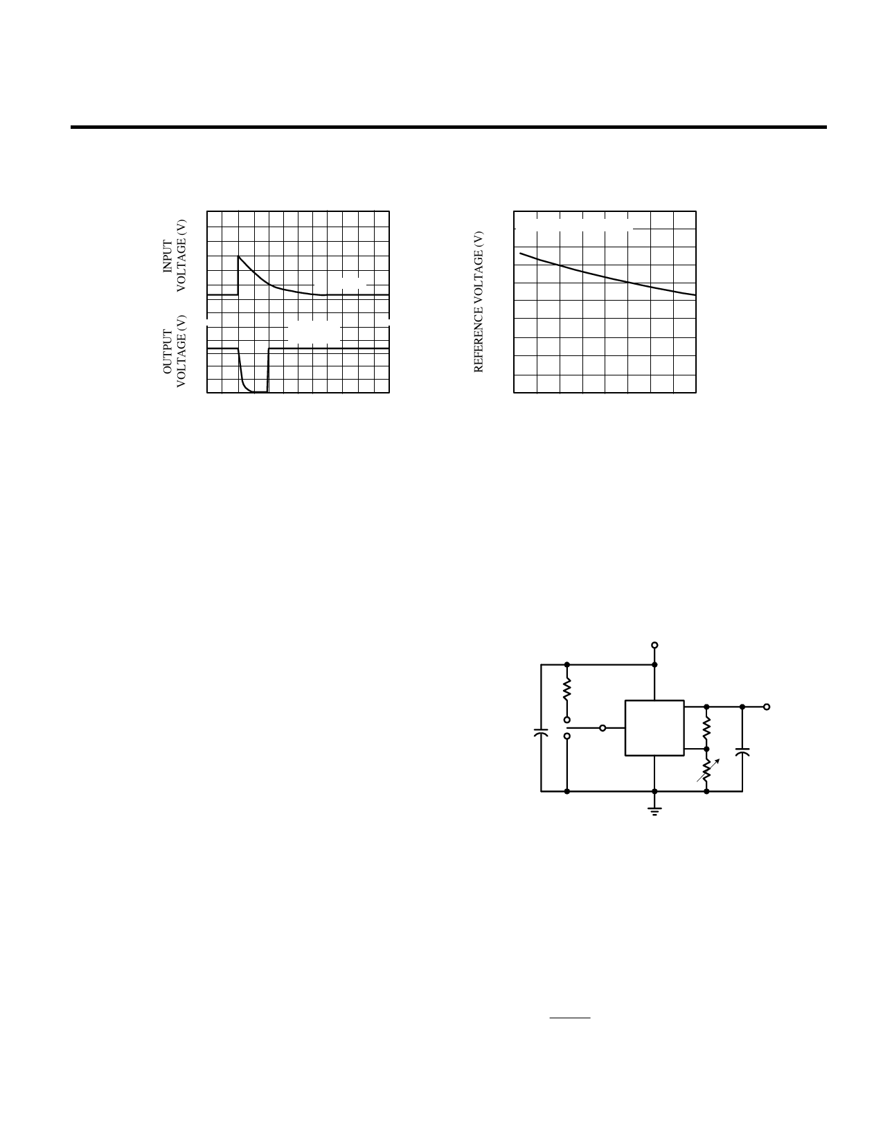
TYPICAL PERFORMANCE CHARACTERISTICS (Continued)
Operation During Load Dump
70
60
50
40
30
20
τ =150 ms
10
0
5
~~
CO= 100µF
~~
4
RL= 500Ω
3
2
1
0
-100 0 100 200 300 400 500
TIME (ms)
Reference Voltage
1.30
1.28 AMS3107 ADJUSTABLE
1.26
1.24
1.22
1.20
1.18
1.16
1.14
1.12
1.10
0
3 6 9 12 15 18 21 24
OUTPUT VOLTAGE (V)
APPLICATION NOTES
Definition of Terms
Dropout Voltage: The input-output voltage differential at which
the circuit stops to regulate against further reduction in input
voltage. Measured when the output voltage has dropped 100mV
from the nominal voltage obtained at 1V input, dropout voltage is
dependent upon load current and junction temperature.
Input Voltage: The DC voltage applied to the input terminal with
respect to ground. Input-Output Differential: The voltage
difference between the unregulated input voltage and the regulated
output voltage for which the regulator will regulate.
Line Regulation: The change in output voltage for a change in
the input voltage. The line regulation is measured under conditions
of low dissipation or by using low duty cycle pulse testing such
that the average chip temperature is not significantly affected.
Load Regulation: The change in output voltage for a change in
load current at constant chip temperature.
Long term stability: Output voltage stability under accelerated
life-test conditions after 1000 hours with maximum rated voltage
and junction temperature.
Output Noise Voltage: The rms AC voltage at the output, with
constant load and no input ripple, measured over a specified
frequency range.
Quiescent Current: That part of the positive input current that
does not contribute to the positive load current. The regulator
ground lead current.
Ripple Rejection: The ratio of the peak-to –peak input ripple
voltage to the peak-to-peak output ripple voltage at specified
frequency.
Temperature Stability of VO: The percentage change in output
voltage for a thermal variation from room temperature to either
temperature extreme.
Most type of tantalum or electrolytic capacitor can be used in the
applications. A critical characteristic of the capacitors is an ESR
value of 5Ω or less and a resonant frequency above 500kHz. The
value of this capacitor can be increased without limits.
For higher loads, the value of the capacitor should be increased,
specialy when the output voltage is set for 2.5V or less. The
AMS3107 lowest fixed output voltage value is 2.0V.
Typical application circuit (adjustable output)
VIN
10µF
100k
OUT
OFF
ON/OFF AMS3107
R1
ADJUSTABLE
28k
ON
ADJ
+
GND
R2
VOUT
C1
22µF
Minimum Load
In circuits using the fixed output voltage versions, minimum load
is not required. For circuits using the adjustable device, the value
of R1 and R2 should be chosen such, that a current of
approximately 40µA flows through the network. The reference
voltage (1.235V) is measured between the adjust pin and VOUT.
The output voltage can be set by the two resistors R1 and R2
using the following equation:
External capacitor
The AMS3107 series require an output capacitor of 10µF or
greater to ensure device stability. Without the capacitor the device
may oscillate.
VO = VREF ⎜⎛ R1 + R2 ⎟⎞
⎝ R1 ⎠
Advanced Monolithic Systems, Inc. www.advanced-monolithic.com Phone (925) 443-0722
Fax (925) 443-0723
Share Link: 