STK11C88-SF45I Просмотр технического описания (PDF) - Unspecified
Номер в каталоге
Компоненты Описание
Список матч
STK11C88-SF45I Datasheet PDF : 15 Pages
| |||
STK11C88
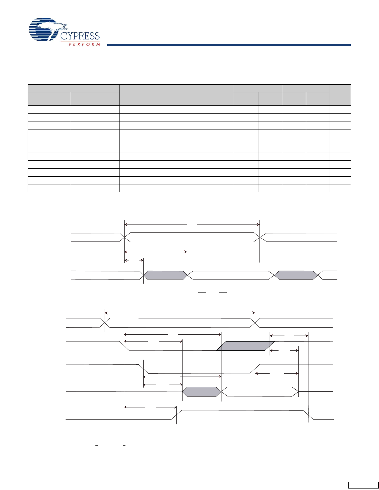
AC Switching Characteristics
SRAM Read Cycle
Parameter
Cypress
Parameter
Alt
tACE
tRC [5]
tAA [6]
tDOE
tOHA [6]
tLZCE [7]
tHZCE [7]
tLZOE [7]
tHZOE [7]
tPU [4]
tPD [4]
tELQV
tAVAV, tELEH
tAVQV
tGLQV
tAXQX
tELQX
tEHQZ
tGLQX
tGHQZ
tELICCH
tEHICCL
Switching Waveforms
Description
Chip Enable Access Time
Read Cycle Time
Address Access Time
Output Enable to Data Valid
Output Hold After Address Change
Chip Enable to Output Active
Chip Disable to Output Inactive
Output Enable to Output Active
Output Disable to Output Inactive
Chip Enable to Power Active
Chip Disable to Power Standby
25 ns
Min
Max
25
25
25
10
5
5
10
0
10
0
25
Figure 5. SRAM Read Cycle 1: Address Controlled [5, 6]
W5&
$''5(66
W$$
W2+$
'4
'$7$287
'$7$9$/,'
45 ns
Unit
Min Max
45
ns
45
ns
45
ns
20
ns
5
ns
5
ns
15
ns
0
ns
15
ns
0
ns
45
ns
Figure 6. SRAM Read Cycle 2: CE and OE Controlled [5]
$''5(66
&(
2(
'4
'$7$287
W5&
W/=&(
W$&(
W'2(
W/=2(
W3'
W+=&(
W+=2(
'$7$9$/,'
W38
$&7,9(
,&&
67$1'%<
Notes
5. WE must be HIGH during SRAM Read Cycles and LOW during SRAM WRITE cycles.
6. I/O state assumes CE and OE < VIL and WE > VIH; device is continuously selected.
7. Measured ±200 mV from steady state output voltage.
Document Number: 001-50591 Rev. **
Page 8 of 15
[+] Feedback
Share Link: 