ST75C530 Просмотр технического описания (PDF) - STMicroelectronics
Номер в каталоге
Компоненты Описание
Список матч
ST75C530
SUPER INTEGRATED DEVICES WITH DSP, AFE & MEMORIES FORTELEPHONY, MODEM, FAX OVERINTERNET & POTS LINES
STMicroelectronics

ST75C530 Datasheet PDF : 84 Pages
| |||
ST75C530 - ST75C540
IV - ELECTRICAL SPECIFICATIONS
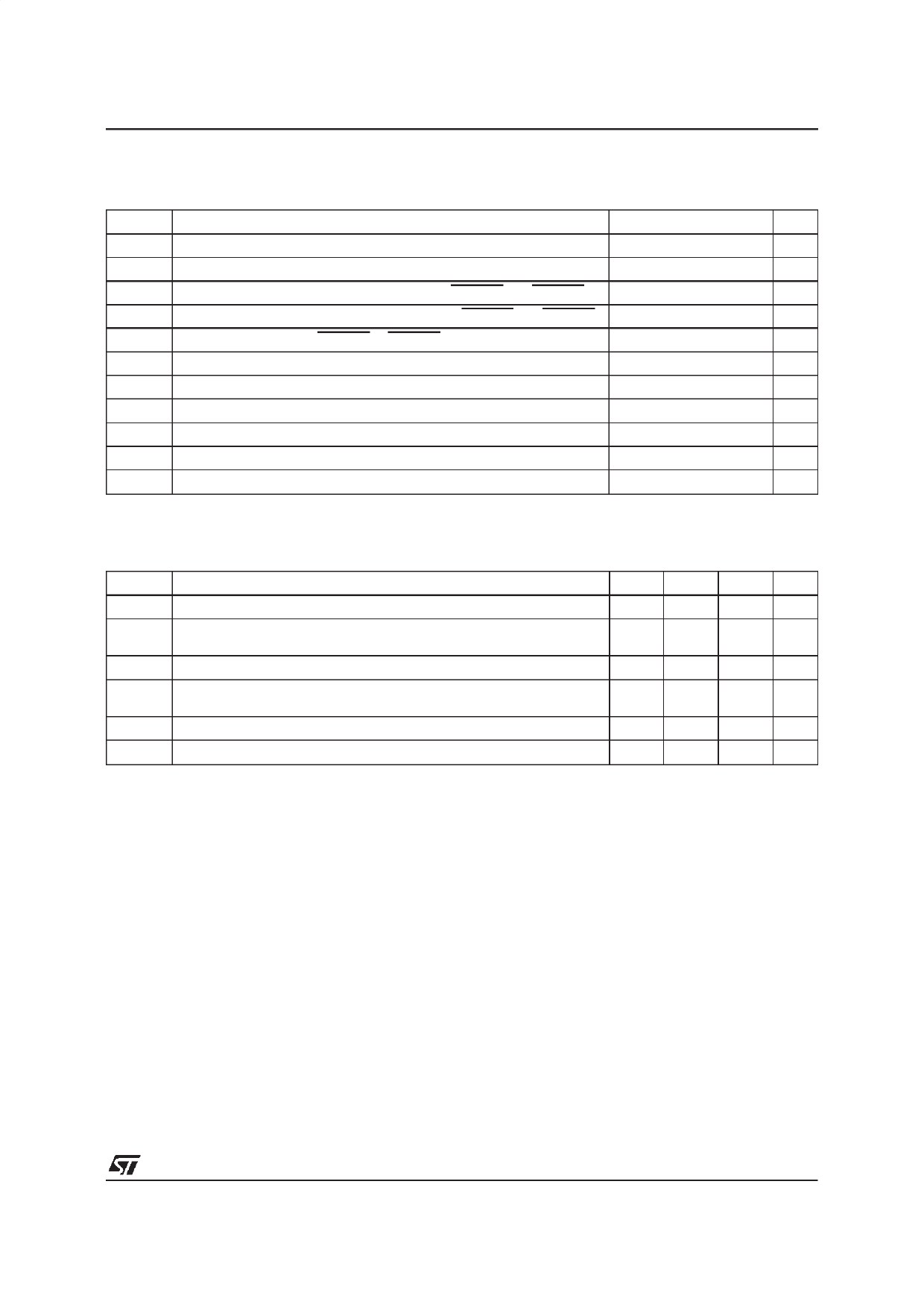
IV.1 - Maximum Ratings (AGND = DGND = RGND = 0V, all voltages with respect to 0V)
Symbol
Parameter
Value
Unit
AVDD Analog Power Supply
-0.3, 6.0
V
DVDD Digital Power Supply
-0.3, 6.0
V
II
Input Current per Pin (except supply pins and RELAY0 and RELAY1)
-10, +10
mA
IO
Output Current per Pin (except supply pins and RELAY0 and RELAY1)
-20, +20
mA
IO2 Output Current per Pin RELAY0 or RELAY1 (respect to RGND)
-40, 0
mA
VIA Analog Input Voltage
-0.3, AVDD + 0.3
V
VID Digital Input Voltage
-0.3, DVDD + 0.3
V
VIDGPIO Digital Input Voltage at GPIO
5.25
V
Toper Operating Temperature
0, +70
°C
Tstg Storage Temperature
- 40, +125
°C
Ptot Maximum Power Dissipation
1500
mW
Warning : Operation beyond these limits may result in permanent damage to the device. Normal operation is not guaranted at these extremes.
IV.2 - Recommended Operating Conditions
(AGND = DGND = RGND = 0V, all voltages with respect to 0V)
Symbol
Parameter
Min. Typ. Max. Unit
VDD Supply Voltage
IDD Supply Current
ST75C530
ST75C540
4.75
5
5.25 V
130 150 mA
145 165 mA
PDLP
PD
Low Power
Power
ST75C530
ST75C540
30 mW
650 790 mW
725 866 mW
VCM Common Mode Voltage Output (refer to AVDD/2)
ICM Common Mode Current (see Note 1)
-5
+5
%
100
µA
Note 1 : DC current only. If dynamic load exists, the VCM output must be buffered or the performances of ADCs and DACs will be degraded.
9/84
Share Link: