MSU2052L40 Просмотр технического описания (PDF) - Mosel Vitelic, Corp
Номер в каталоге
Компоненты Описание
Список матч
MSU2052L40 Datasheet PDF : 21 Pages
| |||
MOSEL VITELIC
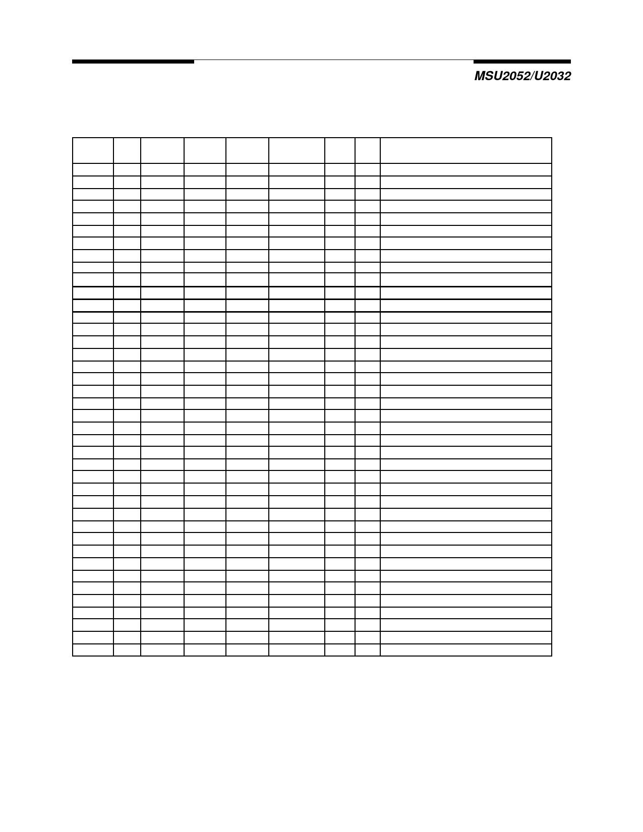
Pin Descriptions
MSU2052/U2032
40 PDIP Dice 44 LQFP
Pin# Pad# Pin#
1
39
40
2
40
41
3
41
42
4
42
43
5
43
44
6
1
1
7
2
2
8
3
3
9
4
4
10
5
5
11
6
7
12
7
8
13
8
9
14
9
10
15
10
11
16
11
12
17
12
13
18
13
14
19
14
15
20 15~17 16
21
18
18
22
19
19
23
20
20
24
21
21
25
22
22
26
23
23
27
24
24
28
25
25
29
26
26
30
27
27
31
28
29
32
29
30
33
30
31
34
31
32
35
32
33
36
33
34
37
34
35
38
35
36
39
36
37
40 37,38
38
44 PQFP 44 PLCC
Pin#
Pin#
40
2
41
3
42
4
43
5
44
6
1
7
2
8
3
9
4
10
5
11
7
13
8
14
9
15
10
16
11
17
12
18
13
19
14
20
15
21
16
22
18
24
19
25
20
26
21
27
22
28
23
29
24
30
25
31
26
32
27
33
29
35
30
36
31
37
32
38
33
39
34
40
35
41
36
42
37
43
38
44
Symbol
T2EX/P1.0
T2/P1.1
P1.2
P1.3
P1.4
P1.5
P1.6
P1.7
RES
RXD/P3.0
TXD/P3.1
#INT0/P3.2
#INT1/P3.3
T0/P3.4
T1/P3.5
#WR/P3.6
#RD/P3.7
XTAL2
XTAL1
VSS
A8/P2.0
A9/P2.1
A10/P2.2
A11/P2.3
A12/P2.4
A13/P2.5
A14/P2.6
A15/P2.7
#PSEN
ALE
#EA
AD7/P0.7
AD6/P0.6
AD5/P0.5
AD4/P0.4
AD3/P0.3
AD2/P0.2
AD1/P0.1
AD0/P0.0
VDD
Active I/O
i/o
i/o
i/o
i/o
i/o
i/o
i/o
i/o
i
i/o
i/o
L/- i/o
L/- i/o
i/o
i/o
L/- i/o
L/- i/o
o
i
i/o
i/o
i/o
i/o
i/o
i/o
i/o
i/o
Lo
Ho
L
i
i/o
i/o
i/o
i/o
i/o
i/o
i/o
i/o
Names
bit 0 of Port 1 & timer 2
bit 1 of Port 1 & timer control
bit 2 of Port 1
bit 3 of Port 1
bit 4 of Port 1
bit 5 of Port 1
bit 6 of Port 1
bit 7 of Port 1
Reset
bit 0 of Port 3 & Receive data
bit 1 of Port 3 & Transmit data
bit 2 of Port 3 & low true Interrupt 0
bit 3 of Port 3 & low true Interrupt 1
bit 4 of Port 3 & Timer 0
bit 5 of Port 3 & Timer 1
bit 6 of Port 3 & Write (low enable)
bit 7 of Port 3 & Read (low enable)
Crystal out
Crystal in
Sink Voltage, Ground
bit 0 of Port 2 & Address 8
bit 1 of Port 2 & Address 9
bit 2 of Port 2 & Address 10
bit 3 of Port 2 & Address 11
bit 4 of Port 2 & Address 12
bit 5 of Port 2 & Address 13
bit 6 of Port 2 & Address 14
bit 7 of Port 2 & Address 15
Program store enable (low enable)
Address latch enable
External access first 8 KB memory
bit 7 of Port 0 & Address or Data 7
bit 6 of Port 0 & Address or Data 6
bit 5 of Port 0 & Address or Data 5
bit 4 of Port 0 & Address or Data 4
bit 3 of Port 0 & Address or Data 3
bit 2 of Port 0 & Address or Data 2
bit 1 of Port 0 & Address or Data 1
bit 0 of Port 0 & Address or Data 0
Drive Voltage, +3 Vcc (or +5 Vcc)
Rev. 1.0 February 1998
4
Share Link: 