LT1680 Просмотр технического описания (PDF) - Linear Technology
Номер в каталоге
Компоненты Описание
Список матч
LT1680 Datasheet PDF : 16 Pages
| |||
U
OPERATION
Slope Compensation
For duty cycles greater than 50%, slope compensation is
required to prevent current mode duty cycle instability in
the regulator control loop. The LT1680 employs internal
slope compensation that is adequate for most applica-
LT1680
tions. However, if additional slope compensation is de-
sired, it is available through the SL/ADJ pin. Excessive
slope compensation will cause reduction in maximum
load current capability and is generally not desirable.
APPLICATIONS INFORMATION
RSENSE Selection for Input Current Limit
RSENSE generates a voltage that is proportional to the
inductor current for use by the LT1680 current sense
amplifier. The value of RSENSE is based on the required
input current. The average current limit function has a
typical threshold of 120mV/RSENSE, or:
RSENSE = 120mV/ILIMIT
Operation with VSENSE common mode voltage below 4.5V
may slightly degrade current limit accuracy. See Average
Current Limit Threshold Tolerance vs Common Mode
Voltage in the Typical Performance Characteristics sec-
tion for more information.
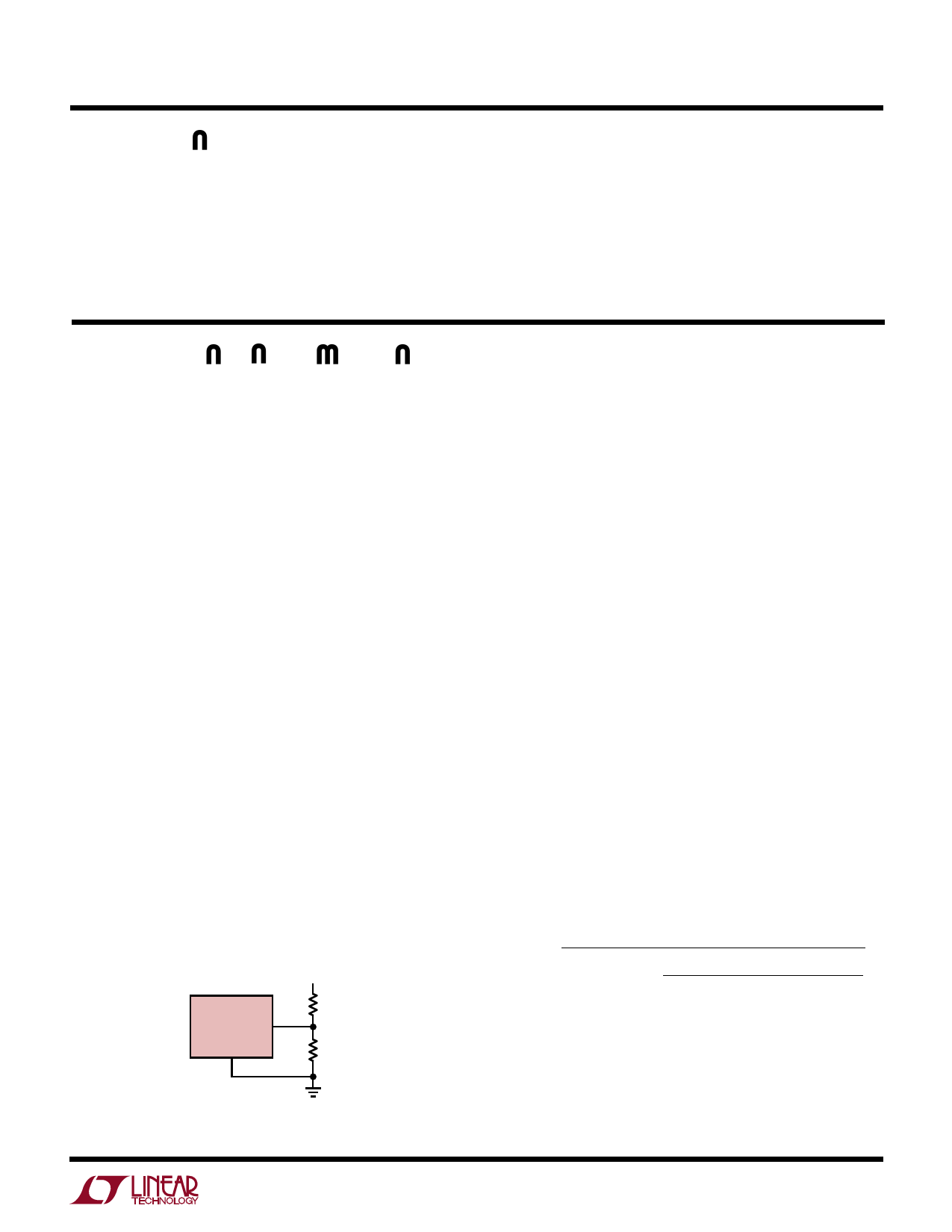
Output Voltage Programming
Output voltage is programmed through a resistor feed-
back network to the VFB pin (Pin 7) on the LT1680. This pin
is the inverting input of the error amplifier, which is
internally referenced to 1.25V. The divider is ratioed to
provide 1.25V at the VFB pin when the output is at its
desired value. Output voltage is thus set following the
relation:
VOUT = 1.25V(1 + R2/R1)
when an external resistor divider is connected to the
output as shown in Figure 1.
VOUT
R2
LT1680
7
VFB
SGND
R1
6
1680 F01
Figure 1. Programming LT1680 Output Voltage
If high value feedback resistors are used, the input bias
current of the VFB pin (1µA maximum) could cause a slight
increase in output voltage. A Thevenin resistance at the
VFB pin of < 5k is recommended.
Oscillator Components RCT and CCT
The LT1680 oscillator creates a modified sawtooth at its
timing node (CT) with a slow charge, rapid discharge
characteristic. The discharge time (tDISCH) corresponds to
the minimum off time of the PWM controller. This limits
maximum duty cycle (DCMAX) to:
DCMAX = 1 – (tDISCH)(fO)
This relation corresponds to the minimum value of the
timing resistor (RCT), which can be determined according
to the following relation (RCT vs DCMAX graph appears in
the Typical Performance Characteristics section):
RCT(MIN) ≈ [(0.8)(10– 3)(1 – DCMAX)] – 1
Values for RCT > 15k yield maximum duty cycles above
90%. Given a timing resistor value, the value of the timing
capacitor (CCT) can then be determined for desired oper-
ating frequency (fO) using the relation:
( () ( ) )( ) ( ) CCT ≈
1/ fO
–
100
10–
9
RCT / 1.85
+
1.75
2.5
10–
3
–
3.375 / RCT
A plot of Operating Frequency vs RCT and CCT is shown in
Figure 2. Typical 100kHz operational values are CCT =
1000pF and RCT = 16.9k.
9
Share Link: 