V29C51001T-45J Просмотр технического описания (PDF) - Mosel Vitelic, Corp
Номер в каталоге
Компоненты Описание
Список матч
V29C51001T-45J Datasheet PDF : 16 Pages
| |||
MOSEL VITELIC
Functional Description
The V29C51001T/V29C51001B consists of 256
equally-sized sectors of 512 bytes each. The 8 KB
lockable Boot Block is intended for storage of the
system BIOS boot code. The boot code is the first
piece of code executed each time the system is
powered on or rebooted.
The V29C51001 is available in two versions: the
V29C51001T with the Boot Block address starting
from 1E000H to 1FFFFH, and the V29C51001B
with the Boot Block address starting from 00000H
to 1FFFFH.
Read Cycle
A read cycle is performed by holding both CE
and OE signals LOW. Data Out becomes valid only
when these conditions are met. During a read cycle
WE must be HIGH prior to CE and OE going LOW.
WE must remain HIGH during the read operation
for the read to complete (see Table 1).
Output Disable
Returning OE or CE HIGH, whichever occurs first
will terminate the read operation and place the l/O
pins in the HIGH-Z state.
Standby
The device will enter standby mode when the CE
signal is HIGH. The l/O pins are placed in the
HIGH-Z, independent of the OE signal.
Command Sequence
The V29C51001T/V29C51001B does not
provide the “reset” feature to return the chip to its
normal state when an incomplete command
V29C51001T/V29C51001B
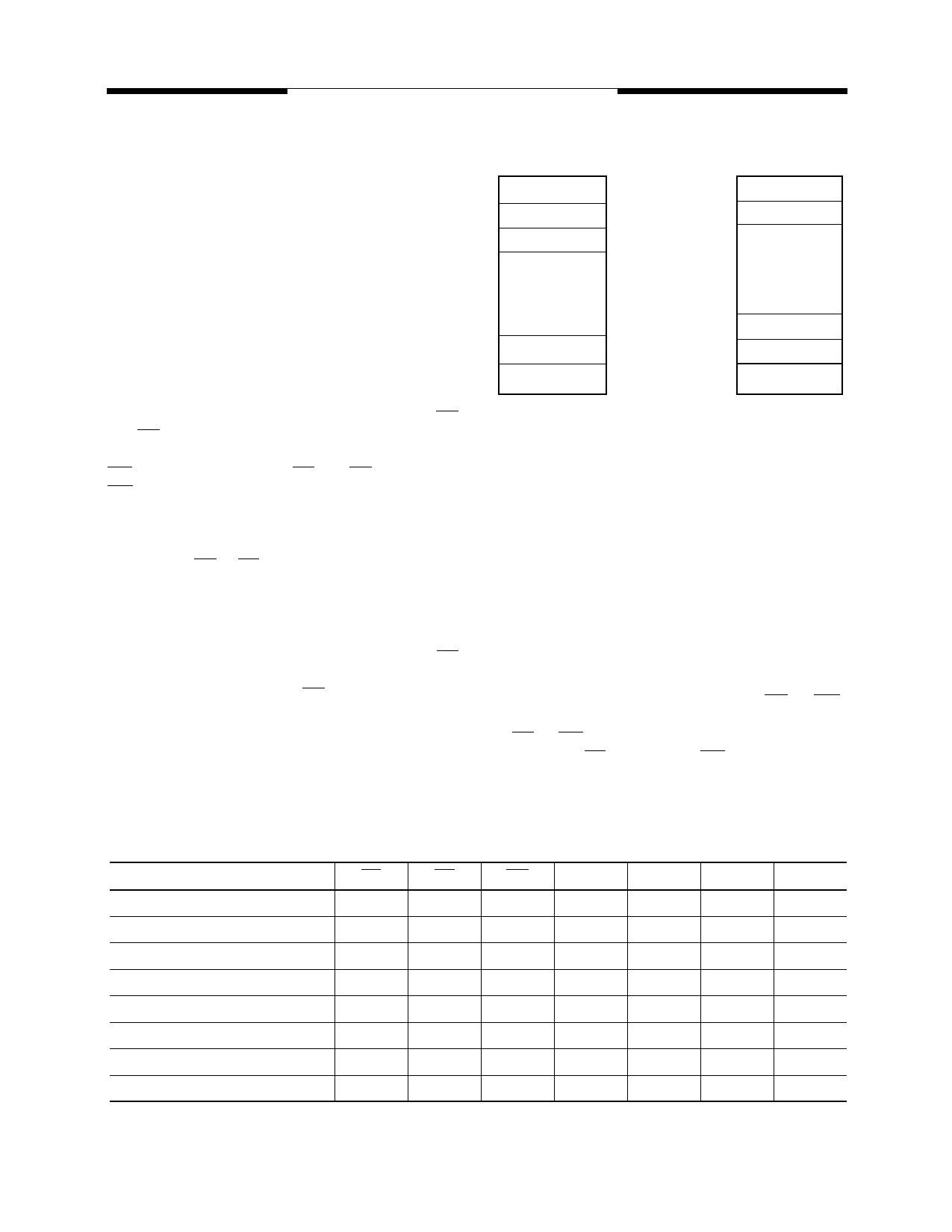
V29C51001T
8KB Boot Block
512
1FFFFH
1E000H
V29C51001B
512
512
512
•
•
•
•
•
•
512
512
512
01FFFH
512
8KB Boot Block
00000H 00000H
51001-13
8KB Boot Block = 16 Sectors
sequence or an interruption has happened. In this
case, normal operation (Read Mode) can be
restored by issuing a “non-existent” command
sequence, for example Address: 5555H, Data FFH.
Byte Program Cycle
The V29C51001T/V29C51001B is programmed
on a byte-by-byte basis. The byte program
operation is initiated by using a specific four-bus-
cycle sequence: two unlock program cycles, a
program setup command and program data
program cycles (see Table 2).
During the byte program cycle, addresses are
latched on the falling edge of either CE or WE,
whichever is last. Data is latched on the rising edge
of CE or WE, whichever is first. The byte program
cycle can be CE controlled or WE controlled.
Table 1. Operation Modes Decoding
Decoding Mode
CE
OE
WE
A0
A1
A9
I/O
Read
VIL
VIL
VIH
A0
A1
A9
READ
Byte Write
VIL
VIH
VIL
A0
A1
A9
PD
Standby
VIH
X
X
X
X
X
HIGH-Z
Autoselect Device ID
VIL
VIL
VIH
VIH
VIL
VH
CODE
Autoselect Manufacture ID
VIL
VIL
VIH
VIL
VIL
VH
CODE
Enabling Boot Block Protection Lock
VIL
VH
VIL
X
X
VH
X
Disabling Boot Block Protection Lock
VH
VH
VIL
X
X
VH
X
Output Disable
VIL
VIH
VIH
X
X
X
HIGH-Z
NOTES:
1. X = Don’t Care, VIH = HIGH, VIL = LOW. VH = 12.5V Max.
2. PD: The data at the byte address to be programmed.
V29C51001T/V29C51001B Rev. 0.8 October 2000
9
Share Link: 