IRFP064V Просмотр технического описания (PDF) - International Rectifier
Номер в каталоге
Компоненты Описание
Список матч
IRFP064V Datasheet PDF : 8 Pages
| |||
IRFP064V
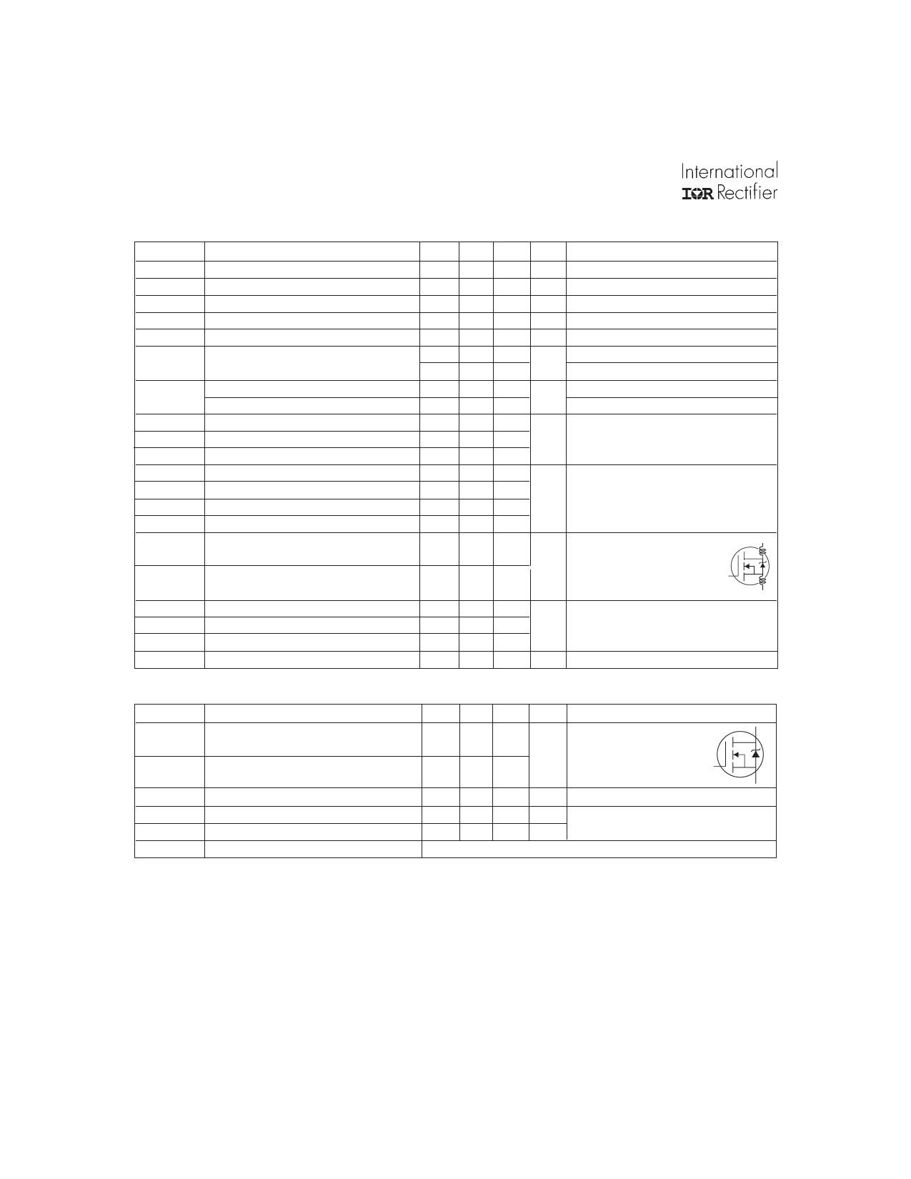
Electrical Characteristics @ TJ = 25°C (unless otherwise specified)
Parameter
V(BR)DSS
∆V(BR)DSS/∆TJ
RDS(on)
VGS(th)
gfs
Drain-to-Source Breakdown Voltage
Breakdown Voltage Temp. Coefficient
Static Drain-to-Source On-Resistance
Gate Threshold Voltage
Forward Transconductance
IDSS
Drain-to-Source Leakage Current
IGSS
Qg
Qgs
Qgd
td(on)
tr
td(off)
tf
Gate-to-Source Forward Leakage
Gate-to-Source Reverse Leakage
Total Gate Charge
Gate-to-Source Charge
Gate-to-Drain ("Miller") Charge
Turn-On Delay Time
Rise Time
Turn-Off Delay Time
Fall Time
LD
Internal Drain Inductance
LS
Internal Source Inductance
Ciss
Coss
Crss
EAS
Input Capacitance
Output Capacitance
Reverse Transfer Capacitance
Single Pulse Avalanche Energy
Min. Typ. Max. Units
Conditions
60 ––– ––– V VGS = 0V, ID = 250µA
––– 0.067 ––– V/°C Reference to 25°C, ID = 1mA
––– ––– 5.5 mΩ VGS = 10V, ID = 78A
2.0 ––– 4.0 V VDS = VGS, ID = 250µA
88 ––– ––– S VDS = 25V, ID = 78A
––– ––– 25 µA VDS = 60V, VGS = 0V
––– ––– 250
VDS = 48V, VGS = 0V, TJ = 150°C
––– ––– 100 nA VGS = 20V
––– ––– -100
VGS = -20V
––– ––– 260
ID = 130A
––– ––– 68 nC VDS = 48V
––– ––– 94
––– 26 –––
VGS = 10V, See Fig. 6 and 13
VDD = 30V
––– 200 ––– ns ID = 130A
––– 100 –––
RG = 4.3Ω
––– 150 –––
VGS = 10V, See Fig. 10
Between lead,
D
––– 5.0 –––
6mm (0.25in.)
nH
from package
G
––– 13 –––
and center of die contact
S
––– 6760 –––
VGS = 0V
––– 1330 –––
VDS = 25V
––– 290 ––– pF ƒ = 1.0MHz, See Fig. 5
––– 1880
310 mJ IAS = 130A, L = 37µH
Source-Drain Ratings and Characteristics
Parameter
IS
Continuous Source Current
(Body Diode)
ISM
Pulsed Source Current
(Body Diode)
VSD
Diode Forward Voltage
trr
Reverse Recovery Time
Qrr
Reverse Recovery Charge
ton
Forward Turn-On Time
Min. Typ. Max. Units
Conditions
MOSFET symbol
D
––– ––– 130
A
showing the
integral reverse
G
––– ––– 520
p-n junction diode.
S
––– ––– 1.2 V TJ = 25°C, IS = 130A, VGS = 0V
––– 94 140 ns TJ = 25°C, IF = 130A
––– 360 540 nC di/dt = 100A/µs
Intrinsic turn-on time is negligible (turn-on is dominated by LS+LD)
Notes:
Repetitive rating; pulse width limited by
max. junction temperature. (See fig. 11)
Starting TJ = 25°C, L = 260µH
RG = 25Ω, IAS = 50A. (See Figure 12)
ISD ≤ 130A, di/dt ≤ 230A/µs, VDD ≤ V(BR)DSS,
TJ ≤ 175°C
Pulse width ≤ 400µs; duty cycle ≤ 2%.
This is a typical value at device destruction and represents
operation outside rated limits.
This is a calculated value limited to TJ = 175°C .
Calculated continuous current based on maximum allowable
junction temperature. Package limitation current is 90A.
2
www.irf.com
Share Link: 