74LVC06A Просмотр технического описания (PDF) - Philips Electronics
Номер в каталоге
Компоненты Описание
Список матч
74LVC06A Datasheet PDF : 16 Pages
| |||
Philips Semiconductors
Hex inverter with open-drain outputs
Product specification
74LVC06A
FEATURES
• 5 V tolerant inputs and outputs (open drain) for
interfacing with 5 V logic
• Wide supply voltage range from 1.65 to 5.5 V
• CMOS low power consumption
• Direct interface with TTL levels
• Inputs accept voltages up to 5 V
• Complies with JEDEC standard no. 8-1A.
DESCRIPTION
The 74LVC06A is a high-performance, low-power,
low-voltage, Si-gate CMOS device, superior to most
advanced CMOS compatible TTL families.
Inputs can be driven from either 3.3 or 5 V devices. This
feature allows the use of these devices as translators in a
mixed 3.3 to 5 V environment.
The 74LVC06A provides six inverting buffers.
The outputs of the 74LVC06A devices are open drain and
can be connected to other open-drain outputs to
implement active-LOW wired-OR or active-HIGH
wired-AND functions.
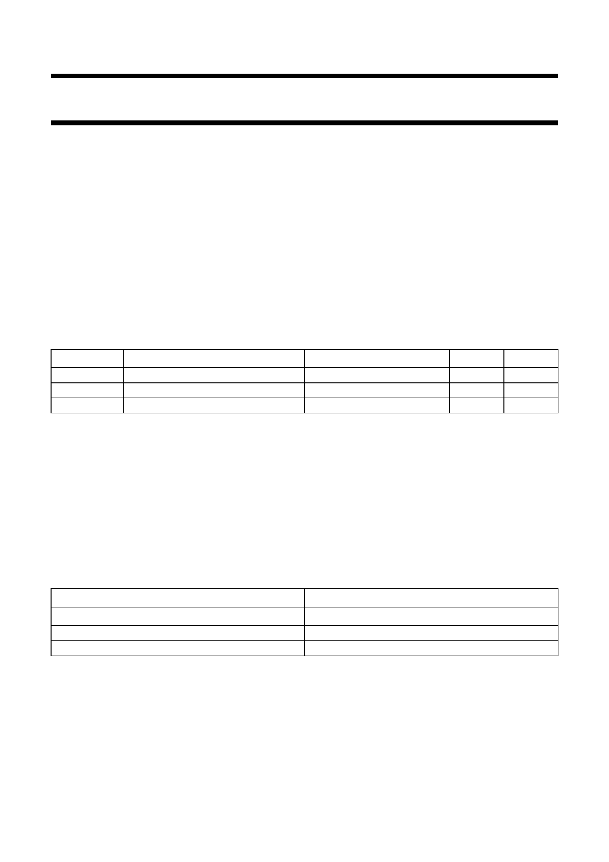
QUICK REFERENCE DATA
GND = 0 V; Tamb = 25 °C; tr = tf ≤ 2.5 ns.
SYMBOL
PARAMETER
CONDITIONS
tPLZ/tPZL
CI
CPD
propagation delay nA to nY
input capacitance
power dissipation capacitance per gate
CL = 50 pF; VCC = 3.3 V
VI = GND to VCC; note 1
Note
1. CPD is used to determine the dynamic power dissipation (PD in µW).
PD = CPD × VCC2 × fi + Σ(CL × VCC2 × fo) where:
fi = input frequency in MHz;
fo = output frequency in MHz;
CL = output load capacitance in pF;
VCC = supply voltage in Volts;
Σ(CL × VCC2 × fo) = sum of the outputs.
TYP.
2.3
5.0
8.0
UNIT
ns
pF
pF
FUNCTION TABLE
See note 1.
INPUT
nA
L
H
Note
1. H = HIGH voltage level;
L = LOW voltage level;
Z = high impedance OFF-state.
OUTPUT
nY
Z
L
2000 Mar 07
2
Share Link: 