WS512K32-XXX Просмотр технического описания (PDF) - Unspecified
Номер в каталоге
Компоненты Описание
Список матч
WS512K32-XXX Datasheet PDF : 11 Pages
| |||
WS512K32-XXX
AC CHARACTERISTICS
(VCC= 5.0V, VSS = 0V, TA= -55°C to +125°C)
Parameter
Read Cycle
Symbol
-15*
-17
-20
-25
-35
-45
-55
Units
Min Max Min Max Min Max Min Max Min Max Min Max Min Max
Read Cycle Time
Address Access Time
Output Hold from Address Change
Chip Select Access Time
Output Enable to Output Valid
Chip Select to Output in Low Z
Output Enable to Output in Low Z
Chip Disable to Output in High Z
Output Disable to Output in High Z
tRC
15
17
20
25
35
45
55
ns
tAA
15
17
20
25
35
45
55 ns
tOH
0
0
0
0
0
0
0
ns
tACS
15
17
20
25
35
45
55 ns
tOE
8
9
10
12
25
25
25 ns
tCLZ1
2
2
2
2
4
4
4
ns
tOLZ1
0
0
0
0
0
0
0
ns
tCHZ1
12
12
12
12
15
20
20 ns
tOHZ1
12
12
12
12
15
20
20 ns
* 15ns Access Time available only in Commercial and Industrial Temperature. This speed is not fully characterized and is subject to change without notice.
1. This parameter is guaranteed by design but not tested.
AC CHARACTERISTICS
(VCC= 5.0V, VSS = 0V, TA= -55°C to +125°C)
Parameter
Symbol
-15*
-17
-20
-25
-35
-45
-55
Units
Write Cycle
Min Max Min Max Min Max Min Max Min Max Min Max Min Max
Write Cycle Time
tWC
15
17
20
25
35
45
55
ns
Chip Select to End of Write
tCW
13
15
15
17
25
35
50
ns
Address Valid to End of Write
tAW
13
15
15
17
25
35
50
ns
Data Valid to End of Write
tDW
10
11
12
13
20
25
25
ns
Write Pulse Width
tWP
13
15
15
17
25
35
40
ns
Address Setup Time
tAS
2
2
2
2
2
2
2
ns
Address Hold Time
tAH
0
0
0
0
0
5
5
ns
Output Active from End of Write
t OW1
2
2
3
4
4
5
5
ns
Write Enable to Output in High Z tWHZ1
8
9
11
13
15
20
20 ns
Data Hold Time
tDH
0
0
0
0
0
0
0
ns
* 15ns Access Time available only in Commercial and Industrial Temperature. This speed is not fully characterized and is subject to change without notice.
1. This parameter is guaranteed by design but not tested.
2 . The Address Setup Time of minimum 2ns is for the G2T, G1U and H1 packages. tAS minimum for the G4T package is 0ns.
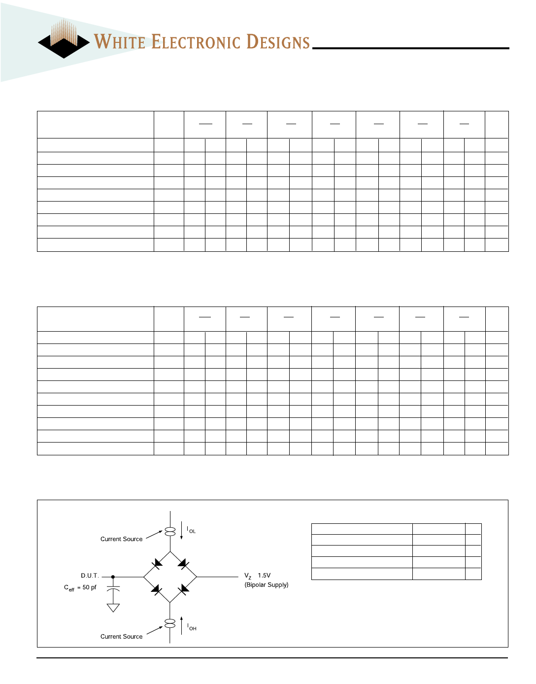
FIG. 4
AC TEST CIRCUIT
AC TEST CONDITIONS
Parameter
Typ
Unit
Input Pulse Levels
VIL = 0, VIH = 3.0 V
Input Rise and Fall
5
ns
Input and Output Reference Level
1.5
V
Output Timing Reference Level
1.5
V
NOTES:
VZ is programmable from -2V to +7V.
IOL & IOH programmable from 0 to 16mA.
Tester Impedance Z0 = 75 ý.
VZ is typically the midpoint of VOH and VOL.
IOL & IOH are adjusted to simulate a typical resistive load circuit.
ATE tester includes jig capacitance.
White Electronic Designs Corporation (602) 437-1520 www.whiteedc.com
4
Share Link: 