UPC1687GV Просмотр технического описания (PDF) - California Eastern Laboratories.
Номер в каталоге
Компоненты Описание
Список матч
UPC1687GV Datasheet PDF : 5 Pages
| |||
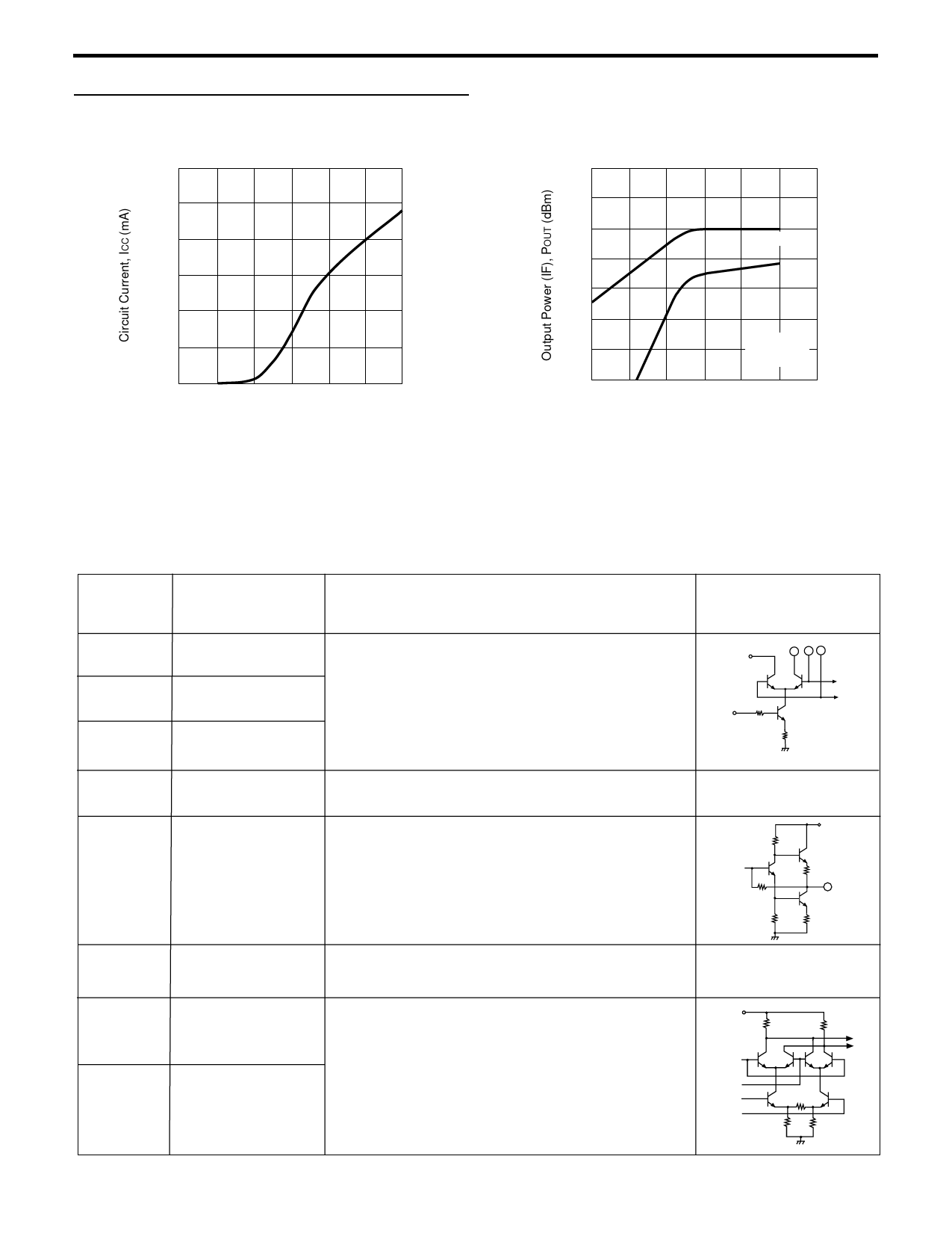
TYPICAL PERFORMANCE CURVES (TA = 25°C)
CIRCUIT CURRENT vs.
SUPPLY VOLTAGE
50
40
30
20
10
0
1
2
3
4
5
6
Supply Voltage, VCC (V)
UPC1687GV
OUTPUT POWER AND
INTERMODULATION DISTORTION
vs. INPUT POWER
+20
POUT
0
IM 3
-20
-40
-40
VCC = 5 V
RF = 500 MHz
IF = 50 MHz
-20
0
+20
Input Power (RF), PIN (dBm)
Each Tone
PIN DESCRIPTION
Pin
Pin
No.
Name
1
OSC Base
(bypass)
2
OSC Base
(feedback)
3
OSC
Collector (Coupling)
4
VCC
5
IF Output
6
GND
7
RF Input 1
(bypass)
8
RF Input 2
Description
Input pins for the internal oscillator which consists
of a balanced amplifier. Pin 1 should be bypassed to ground
through a capacitor. Pins 2 and 3 should be externally
equipped with a tank resonator. Note that pin 3 is an open
collector and must be supplied voltage through an external
resistor or choke coil.
Internal
Equivalent
Circuit
VCC
VREF
3 12
to OSC
Buffer
Amp
Supply voltage pin. This pin should be externally equipped
with a bypass capacitor to minimize ground impedance.
IF output pin from the single-ended push-pull amplifier.
This pin is an emitter follower output with a constant
resistive impedance of 50 Ω.
from IF
Pre amp
Ground pin. This pin must be connected to system ground.
Form ground pattern as wide as possible to minimize
ground impedance.
VCC
RF input pins. Pins 7 and 8 are each base inputs to a
double balanced mixer. Either pin can be assigned as the
from
input. The unused pin should be bypassed to ground
OSC
Buffer
through a capacitor.
RF
Inputs
VCC
5
IF
Output
to IF
Amp
Share Link: 