LT1572 Просмотр технического описания (PDF) - Linear Technology
Номер в каталоге
Компоненты Описание
Список матч
LT1572 Datasheet PDF : 12 Pages
| |||
LT1572
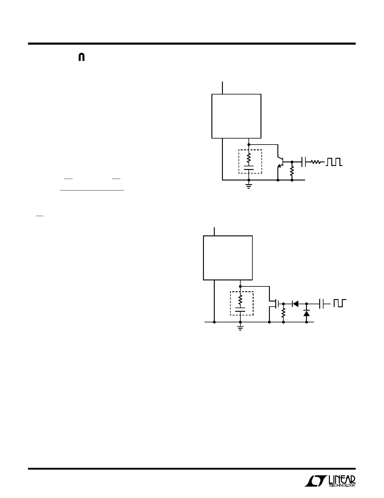
OPERATIO
Synchronizing
The LT1572 can be externally synchronized in the fre-
quency range of 120kHz to 160kHz. This is accomplished
as shown in the accompanying figures. Synchronizing
occurs when the VC pin is pulled to ground with an external
transistor. To avoid disturbing the DC characteristics of
the internal error amplifier, the width of the synchronizing
pulse should be under 0.3µs. C2 sets the pulse width at ≅
0.2µs. The effect of a synchronizing pulse on the LT1572
amplifier offset can be calculated from:
( )( ) ∆VOS
=
KT
q
tS
fS
IC
+
RVC3
IC
KT
q
=
26mV
at
25°C
tS = pulse width
fS = pulse frequency
IC = VC source current (≈ 200µA)
VC = operating VC voltage (1V to 2V)
R3 = resistor used to set mid-frequency “zero”
in frequency compensation network.
With tS = 0.2µs, fS = 150kHz, VC = 1.5V, and R3 = 2k, offset
voltage shift is ≈ 3.8mV. This is not particularly bother-
some, but note that high offsets could result if R3 were
reduced to a much lower value. Also, the synchronizing
transistor must sink higher currents with low values of R3,
so larger drives may have to be used. The transistor must
be capable of pulling the VC pin to within 200mV of ground
to ensure synchronizing.
Synchronizing with Bipolar Transistor
VIN
LT1572
GND
VC
R3
2N2369
C1
C2
39pF R1
3k
R2
FROM 5V
2.2k
LOGIC
1572 OP01
Synchronizing with MOS Transistor
VIN
LT1572
GND
VC
R3
VN2222*
C1
D1
1N4158
C2
100pF
R2
D2
FROM 5V
2.2k
1N4158 LOGIC
*SILICONIX OR EQUIVALENT
1572 OP02
10
Share Link: 