PSB4595 Просмотр технического описания (PDF) - Siemens AG
Номер в каталоге
Компоненты Описание
Список матч
PSB4595 Datasheet PDF : 104 Pages
| |||
PSB 4595 / PSB 4596
Analog Line Interface Solution
Pin Definition and Functions
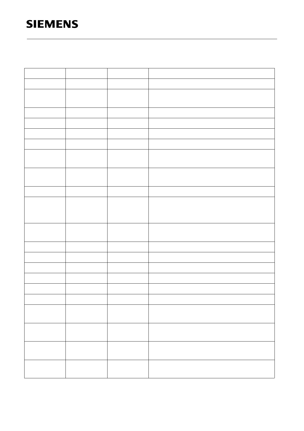
2.2 Pin Definition of ALIS-A PSB 4595
Pin No.
22
24
4
5
6
7
23
19
21
3
1
2
18
17
8
9
16
13
12
11
10
Symbol
VDDA
GNDA
Function
Power
Power
TIP
I
TIP_AC
I
RING
I
RING_AC I
T1G
O
T2G
O
VDD_SENS I
VREF
I/O
CAP1
I/O
CAP2
I/O
SI_0
I
SI_1
I
SO_0
O
SO_1Q
O
TEST
I
CAP_A21 I
CAP_A22 I
CAP_B21 O
CAP_B22 O
Descriptions
Programmable supply for the circuitry
Analog ground: All signals are referred to
this pin
TIP AC+DC sense input
TIP AC sense input
RING AC+DC sense input
RING AC sense input
Gate for external transistor T1 (AC/DC
control)
Gate for external transistor T2 (VDDA
control)
VDDA sense input
Reference voltage: Must be connected to
GNDA via an external capacitor of more
than 10 nF (typ. 15 nF)
Pin for external capacitor of more than 1
µF for DC filtering to pin Cap2
See Cap1
Auxiliary input pin 0
Auxiliary input pin 1
Auxiliary output pin 0
Auxiliary output pin 1
Must be connected permanently to GNDA
Must be connected via a capacitor of more
than 5pF to CAP_A11.
Must be connected via a capacitor of more
than 5pF to CAP_A12.
Must be connected via a capacitor of more
than 5pF to CAP_B11.
Must be connected via a capacitor of more
than 5pF to CAP_B12.
Semiconductor Group
11
Data Sheet 06.98
Share Link: 