PHB3N60E Просмотр технического описания (PDF) - Philips Electronics
Номер в каталоге
Компоненты Описание
Список матч
PHB3N60E Datasheet PDF : 9 Pages
| |||
Philips Semiconductors
PowerMOS transistors
Avalanche energy rated
Product specification
PHP3N60E, PHB3N60E
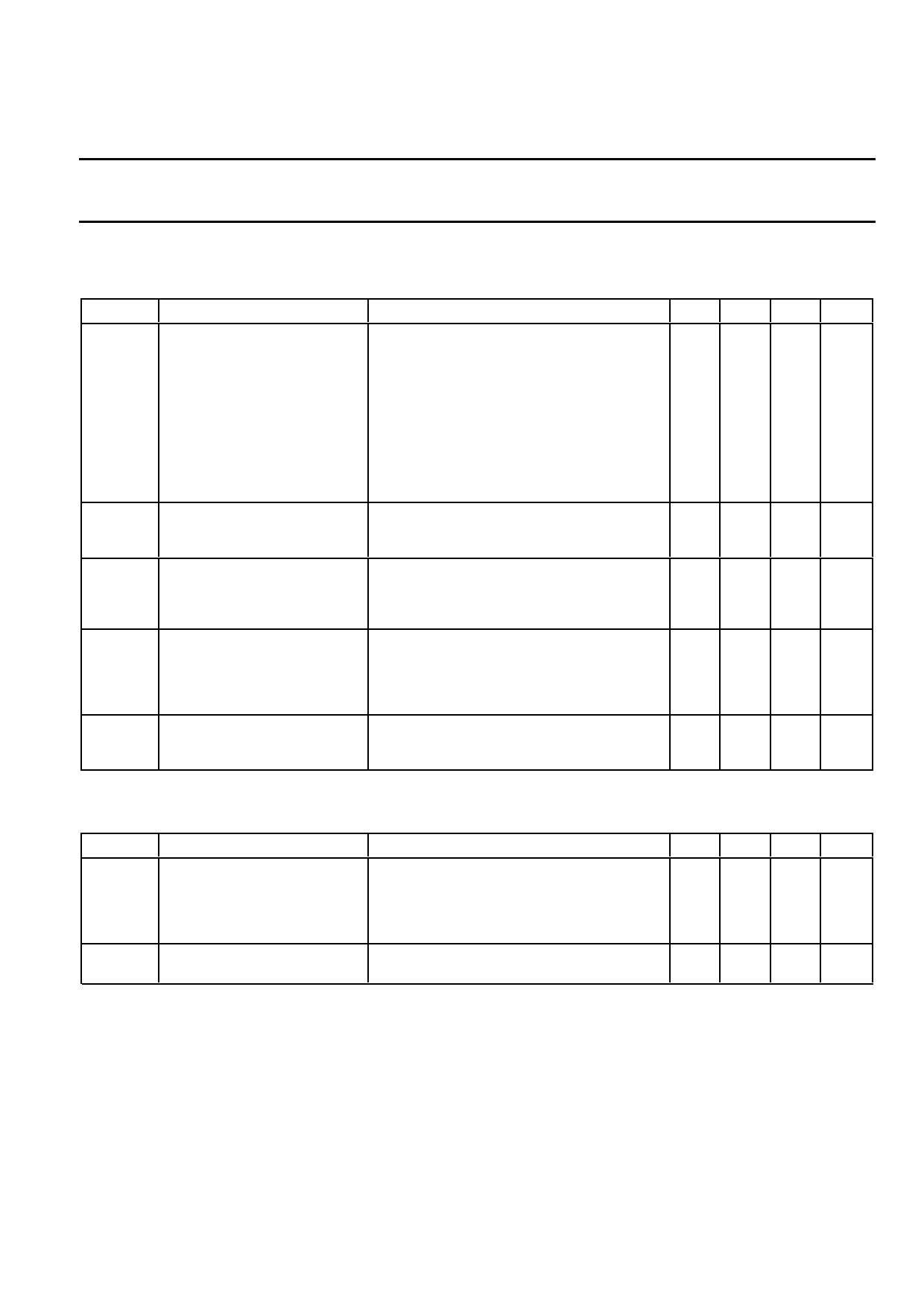
ELECTRICAL CHARACTERISTICS
Tj = 25 ˚C unless otherwise specified
SYMBOL PARAMETER
CONDITIONS
V(BR)DSS Drain-source breakdown
voltage
VGS = 0 V; ID = 0.25 mA
∆V(BR)DSS / Drain-source breakdown
∆Tj
voltage temperature
coefficient
VDS = VGS; ID = 0.25 mA
RDS(ON)
VGS(TO)
gfs
IDSS
IGSS
Drain-source on resistance VGS = 10 V; ID = 1.4 A
Gate threshold voltage
VDS = VGS; ID = 0.25 mA
Forward transconductance VDS = 30 V; ID = 1.4 A
Drain-source leakage current VDS = 600 V; VGS = 0 V
VDS = 480 V; VGS = 0 V; Tj = 125 ˚C
Gate-source leakage current VGS = ±30 V; VDS = 0 V
Qg(tot)
Qgs
Qgd
Total gate charge
Gate-source charge
Gate-drain (Miller) charge
ID = 2.8 A; VDD = 480 V; VGS = 10 V
td(on)
Turn-on delay time
tr
Turn-on rise time
td(off)
Turn-off delay time
tf
Turn-off fall time
VDD = 300 V; RD = 100 Ω;
RG = 18 Ω
Ld
Internal drain inductance Measured from tab to centre of die
Ld
Internal drain inductance Measured from drain lead to centre of die
(SOT78 package only)
Ls
Internal source inductance Measured from source lead to source
bond pad
Ciss
Input capacitance
Coss
Output capacitance
Crss
Feedback capacitance
VGS = 0 V; VDS = 25 V; f = 1 MHz
MIN. TYP. MAX. UNIT
600 -
-
V
- 0.1 - %/K
-
4 4.4 Ω
2.0 3.0 4.0 V
0.7 1.7 -
S
-
1 100 µA
- 50 500 µA
- 10 200 nA
- 25 30 nC
-
2
3 nC
- 12 15 nC
- 10 - ns
- 26 - ns
- 66 - ns
- 30 - ns
- 3.5 - nH
- 4.5 - nH
- 7.5 - nH
- 300 - pF
- 43 - pF
- 25 - pF
SOURCE-DRAIN DIODE RATINGS AND CHARACTERISTICS
Tj = 25 ˚C unless otherwise specified
SYMBOL PARAMETER
CONDITIONS
IS
Continuous source current Tmb = 25˚C
(body diode)
ISM
Pulsed source current (body Tmb = 25˚C
diode)
VSD
Diode forward voltage
IS = 2.8 A; VGS = 0 V
trr
Reverse recovery time
IS = 2.8 A; VGS = 0 V; dI/dt = 100 A/µs
Qrr
Reverse recovery charge
MIN. TYP. MAX. UNIT
-
- 2.8 A
-
- 11 A
-
- 1.2 V
- 500 - ns
-
3
- µC
December 1998
3
Rev 1.200
Share Link: 