MX93521 Просмотр технического описания (PDF) - Macronix International
Номер в каталоге
Компоненты Описание
Список матч
MX93521 Datasheet PDF : 57 Pages
| |||
MX93521
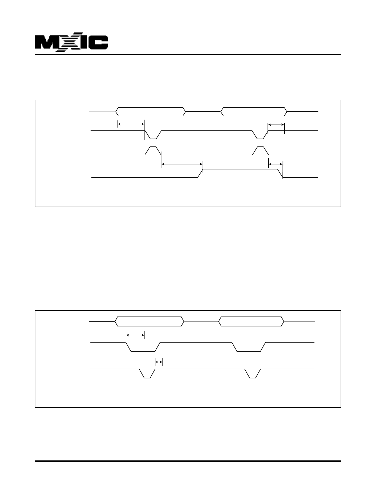
5.1.2 Timing Diagrams
HOST Write Timing (Parallel Mode)
PHDB0-7
ts
th
PHWRB\
SCLK
(INT1\)
RxCmd
tp
tp
HOST Write Timing (Parallel Mode)
HOST should cycle PHWRB\ after writing data to PHDB0-7.
MX93521 will read data from PHDB0-7 on the falling edge of SCLK (rising edge of PHWRB\).
Rxcmd will be toggled if command byte has been processed by MX93521
The PHWRB\ signal will cause MX93521 to latch data from bus PHDB0-7 to MX93521 internal register.The invertted
signal of PHWRB\ will trigger MX93521 INT1\ to read and process the received data byte from internal register. Due
to the interrupt contention, there might be an up to 50 us delay between the rising edge of PHWRB\ and INT1\
actually being served. To keep from command overrun, HOST should check if RxCmd toggled or wait 50 usec before
sending next command byte to MX93521.
HOST Read Timing (Parallel Mode)
PHDB0-7
PACKB\
PHRDB\
ts
ta
HOST Read Timing (Parallel Mode)
When MX93521 write data to PHDB0-7, PACKB\ will become low. HOST needs to poll the status of PACKB\ continu-
ously. When HOST detect low state on PACKB\, HOST should read out data from PHDB0-7. After HOST read the
data from PHDB0-7, PACKB\ will be reset to high.
The maxima delay between MX93521 write data to PHDB0-7 and PACKB\ become low is 10 ns.
The maxima delay between rising edge of PHRDB\ and PACKB\ become high is also 10 ns.
P/N:PM0426
REV. 2.2, JAN 20, 1998
10
Share Link: 