ML145506 Просмотр технического описания (PDF) - LANSDALE Semiconductor Inc.
Номер в каталоге
Компоненты Описание
Список матч
ML145506 Datasheet PDF : 20 Pages
| |||
ML145506
LANSDALE Semiconductor, Inc.
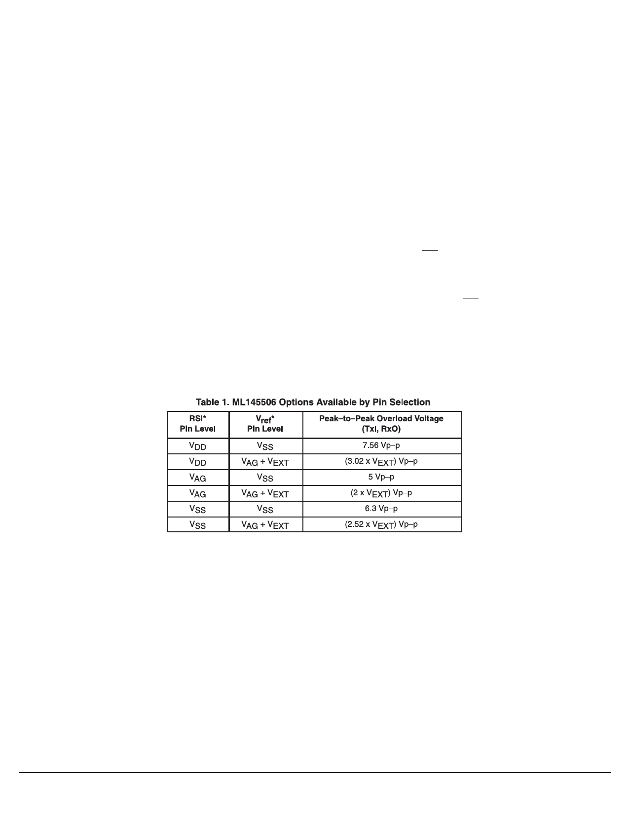
of 1.0, such that a 3 dBm0 signal at TxI corresponds to the peak
converter reference voltage as described in the Vref and RSI pin
descriptions. For a 3.15 V reference, the 3 dBm0 input should be 6.3
V peak–to–peak.
+Tx/ –Tx
Positive Tx Amplifier Input
Negative Tx Amplifier Input
The Txl pin is the input to the transmit band–pass filter. If +Tx or
–Tx is available, then there is an internal amplifier preceding the fil-
ter whose pins are +Tx, –Tx, and TxI. These pins allow access to the
amplifier terminals to tailor the input gain with external resistors.
The resistors should be in the range of 10 kΩ.
POWER SUPPLIES
VDD
Most Positive Power Supply
VDD is typically 5 V to 12 V.
VSS
Most Negative Power Supply
VSS is typically 10 V to 12 V negative of VDD. For a ±5 V
dual–supply system, the typical power supply configuration is
VDD = 5 V, VSS = –5 V, VLS = 0 V (digital ground accommodat-
ing TTL logic levels), and VAG = 0 V being tied to system analog
ground.
For single–supply applications, typical power supply configura-
tions include:
VDD = 10 V to 12 V
VSS = 0 V
VAG generates a mid supply voltage for referencing all analog
signals.
VLS controls the logic levels. This pin should be connected to
VDD for CMOS logic levels from VSS to VDD. This pin should be
connected to digital ground for true TTL logic input levels refer-
enced to VLS, with HCMOS output levels from VLS to VDD.
TESTING CONSIDERATIONS
An analog test mode is activated by connecting MSI and CCI to
128 kHz. In this mode, the input of the A/D (the output of the Tx
filter) is available at the PDI pin. This input is direct coupled to the
A/D side of the codec. The A/D is a differential design. This results
in the gain of this input being effectively attenuated by half. If moni-
tored with a high–impedance buffer, the output of the Tx low–pass
filter can also be measured at the PDI pin. This test mode allows
independent evaluation of the transmit low–pass filter and A/D side
of the codec. The transmit and receive channels of these devices are
tested with the codec–filter fully functional.
Page 10 of 20
www.lansdale.com
Issue A
Share Link: 