LY621024GV Просмотр технического описания (PDF) - Lyontek Inc.
Номер в каталоге
Компоненты Описание
Список матч
LY621024GV Datasheet PDF : 16 Pages
| |||
®
Rev. 1.5
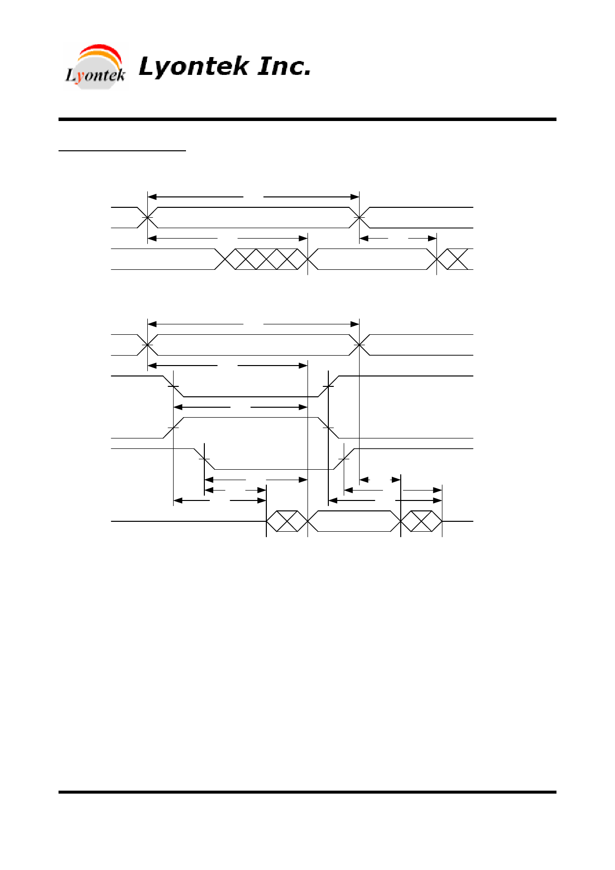
TIMING WAVEFORMS
READ CYCLE 1 (Address Controlled) (1,2)
Address
Dout
tRC
tAA
Previous Data Valid
LY621024
128K X 8 BIT LOW POWER CMOS SRAM
tOH
Data Valid
READ CYCLE 2 (CE# and CE2 and OE# Controlled) (1,3,4,5)
Address
CE#
CE2
tRC
tAA
tACE
OE#
Dout
High-Z
tOE
tOLZ
tCLZ
tOH
tOHZ
tCHZ
Data Valid
High-Z
Notes :
1.WE# is high for read cycle.
2.Device is continuously selected OE# = low, CE# = low., CE2 = high.
3.Address must be valid prior to or coincident with CE# = low, CE2 = high; otherwise tAA is the limiting parameter.
4.tCLZ, tOLZ, tCHZ and tOHZ are specified with CL = 5pF. Transition is measured ±500mV from steady state.
5.At any given temperature and voltage condition, tCHZ is less than tCLZ , tOHZ is less than tOLZ.
Lyontek Inc. reserves the rights to change the specifications and products without notice.
5F, No. 2, Industry E. Rd. IX, Science-Based Industrial Park, Hsinchu 300, Taiwan.
TEL: 886-3-6668838
FAX: 886-3-6668836
6
Share Link: 