LY621024LV Просмотр технического описания (PDF) - Lyontek Inc.
Номер в каталоге
Компоненты Описание
Список матч
LY621024LV Datasheet PDF : 16 Pages
| |||

®
Rev. 1.5
LY621024
128K X 8 BIT LOW POWER CMOS SRAM
FEATURES
Fast access time : 35/55/70ns
Low power consumption:
Operating current : 24/17/15mA (TYP.)
Standby current : 2μA@5V(TYP.) LL/SL version
0.8μA@3V(TYP.) SL version
Single 5V power supply
All inputs and outputs TTL compatible
Fully static operation
Tri-state output
Data retention voltage : 1.5V (MIN.)
Green package available
Package : 32-pin 450 mil SOP
32-pin 600 mil P-DIP
32-pin 8mm x 20mm TSOP-I
32-pin 8mm x 13.4mm STSOP
36-ball 6mm x 8mm TFBGA
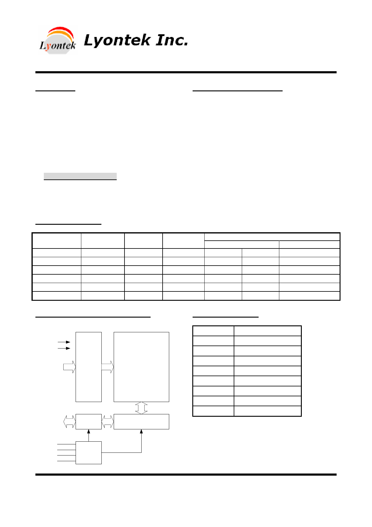
PRODUCT FAMILY
GENERAL DESCRIPTION
The LY621024 is a 1,048,576-bit low power CMOS
static random access memory organized as 131,072
words by 8 bits. It is fabricated using very high
performance, high reliability CMOS technology. Its
standby current is stable within the range of
operating temperature.
The LY621024 is well designed for very low power
system applications, and particularly well suited for
battery back-up nonvolatile memory application.
The LY621024 operates from a single power
supply of 5V and all inputs and outputs are fully TTL
compatible
Product
Family
LY621024(LL)
LY621024(LLE)
LY621024(LLI)
LY621024(SL)
LY621024(SLE)
LY621024(SLI)
Operating
Temperature
0 ~ 70℃
-20 ~ 80℃
-40 ~ 85℃
0 ~ 70℃
-20 ~ 80℃
-40 ~ 85℃
Vcc Range
4.5 ~ 5.5V
4.5 ~ 5.5V
4.5 ~ 5.5V
4.5 ~ 5.5V
4.5 ~ 5.5V
4.5 ~ 5.5V
Speed
35/55/70ns
35/55/70ns
35/55/70ns
35/55/70ns
35/55/70ns
35/55/70ns
Power Dissipation
Standby(ISB1,TYP.) Operating(Icc,TYP.)
-
2µA@5V
24/17/15mA
-
2µA@5V
24/17/15mA
-
2µA@5V
24/17/15mA
0.8µA@3V 2µA@5V
24/17/15mA
0.8µA@3V 2µA@5V
24/17/15mA
0.8µA@3V 2µA@5V
24/17/15mA
FUNCTIONAL BLOCK DIAGRAM
PIN DESCRIPTION
Vcc
Vss
A0-A16
DECODER
128Kx8
MEMORY ARRAY
DQ0-DQ7
I/O DATA
CIRCUIT
COLUMN I/O
SYMBOL
A0 - A16
DQ0 – DQ7
CE#, CE2
WE#
OE#
VCC
VSS
NC
DESCRIPTION
Address Inputs
Data Inputs/Outputs
Chip Enable Inputs
Write Enable Input
Output Enable Input
Power Supply
Ground
No Connection
CE#
CE2
WE#
OE#
CONTROL
CIRCUIT
Lyontek Inc. reserves the rights to change the specifications and products without notice.
5F, No. 2, Industry E. Rd. IX, Science-Based Industrial Park, Hsinchu 300, Taiwan.
TEL: 886-3-6668838
FAX: 886-3-6668836
1