LV71081E Просмотр технического описания (PDF) - SANYO -> Panasonic
Номер в каталоге
Компоненты Описание
Список матч
LV71081E Datasheet PDF : 31 Pages
| |||
LV71081E
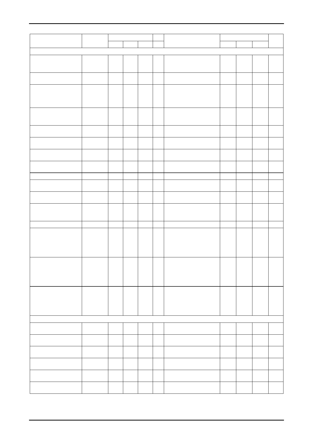
Continued from preceding page.
Parameter
Video Driver part
Symbol
Input signal
Out
Point Signal Freq Point
Test condition
Ratings
Unit
min
typ
max
Output voltage 1
Output voltage 2
Voltage gain 1
VDCD1
95
97
99
VDCD2
93
VGD
Frequency characteristics 1 VFD1
Frequency characteristics 2 VFD2
Frequency characteristics 3 VFD3
Frequency characteristics 4 VFD4
Group delay
VGDD1
Mute attenuation
Differential Gain
Differential Phase
Cross-talk
VMUD
DG1
91
93
DP1
91
93
CTD
Picture S/N
Maximum output level 1
VSND
VOMAXD1
Maximum output level 2
VOMAXD2
Maximum output level 3
VOMAXD3
Sync-SEP part
9 RGB (Pedestal)
0.3
12
17
14 Y (Sync tip)
0.5
23
100k
VIN = 1Vp-p, Line output : 2
5.5
drives, Scart output: DC
directly-coupled single drive
Note 1)
VIN = 1Vp-p,
-1.5
f = 6MHz/100kHz when
6MHzLPF is selected
f = 27MHz/100kHz when
6MHzLPF is selected
f = 12MHz/100kHz when
-1.5
12MHzLPF is selected
f = 54MHz/100kHz when
12MHzLPF is selected
f = 6MHz/100kHz when
6MHzLPF is selected
VIN = 1Vp-p, f=4.43MHz
23 VIN = Video : 1Vp-p
-1
23 VIN = Video : 1Vp-p
-1.5
4.43M
VIN = 1Vp-p, f = 4.43MHz,
Driver output terminated with
75Ω
VIN = Video (50%White)
9 Output level when the linearity
2.8
12 of pins 9, 12, and 17 exceeds
17 1%.
VIN = Linearity (lamp) signal
Output level at linearity 1%
14 Output level when the linearity
2.6
19 of pins 14, 19, and 23 exceeds
23 1%
VIN = Linearity (lamp) signal
Output level at linearity 1%
7 Output level at which the
2.0
11 linearity of pins 7, 11, and 22
22 exceeds 1%
VIN = sin 10kHz
Output level at linearity 1%
0.5
0.7 V
0.7
0.9 V
6.0
6.5 dB
0.0 +1.5 dB
-35
-25 dB
0.0 +1.5 dB
-40
-30 dB
20
35 ns
-60
-50 dB
0
+1 %
0 +1.5 °C
-60
-50 dB
-70
-65 dB
3.0
Vp-p
2.8
Vp-p
2.5
Vp-p
C.SYNC output
High voltage
C.SYNC output
Low voltage
C.SYNC output
delay time
C.SYNC output
pulse width
V.SYNC output
High voltage
V.SYNC output
Low voltage
VCSH
VCSL
TDCS
TWCS
VVSH
VVSL
86
86
86 Note 2)
86 Note 2)
82
82
4.3
4.7
5.0 V
0
0.3
0.6 V
1.0
1.7
2.4 μs
3.2
4.2
5.2 μs
4.3
4.7
5.0 V
0
0.3
0.6 V
Note 1) The Line output can drive two systems through capacitive coupling while the Scart output drives only one system through DC direct coupling.
Note 2) When pin 10 is open
Continued on next page.
No.A1610-3/31
Share Link: 