FM25C160B Просмотр технического описания (PDF) - Cypress Semiconductor
Номер в каталоге
Компоненты Описание
Список матч
FM25C160B Datasheet PDF : 14 Pages
| |||
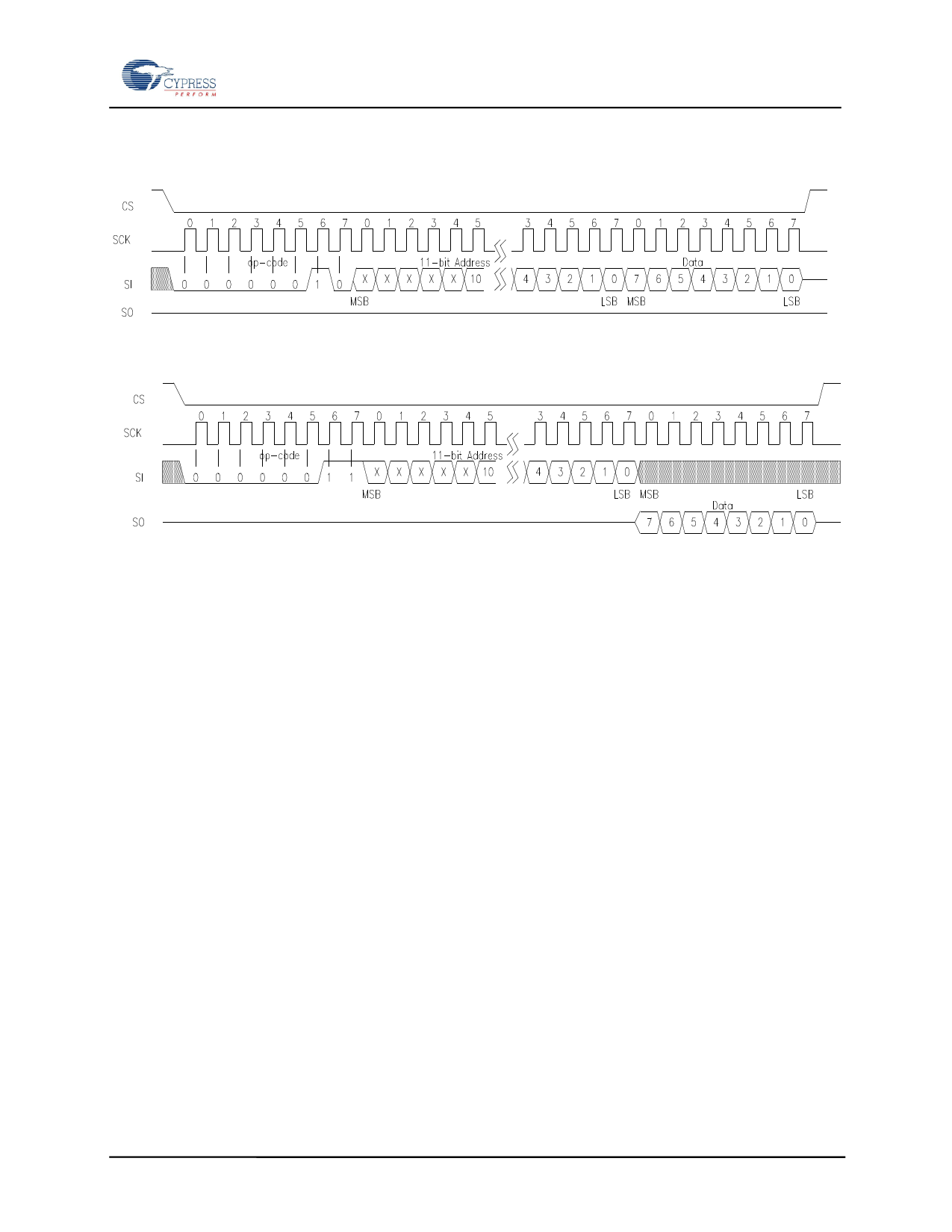
FM25C160B - 16Kb 5V SPI F-RAM
Figure 9. Memory Write
Figure 10. Memory Read
Endurance
Internally, a F-RAM operates with a read and restore
mechanism. Therefore, endurance cycles are applied
for each access: read or write. The F-RAM
architecture is based on an array of rows and
columns. Each access causes a cycle for an entire
row. In the FM25C160B, a row is 64 bits wide.
Every 8-byte boundary marks the beginning of a new
row. Endurance can be optimized by ensuring
frequently accessed data is located in different rows.
Regardless, F-RAM read and write endurance is
effectively unlimited at the 20MHz clock speed.
Even at 2000 accesses per second to the same row, 15
years time will elapse before 1012 endurance cycles
occur.
Document Number: 001-84472 Rev. *A
Page 8 of 14
Share Link: 