W51300 Просмотр технического описания (PDF) - Winbond
Номер в каталоге
Компоненты Описание
Список матч
W51300 Datasheet PDF : 12 Pages
| |||
W51300
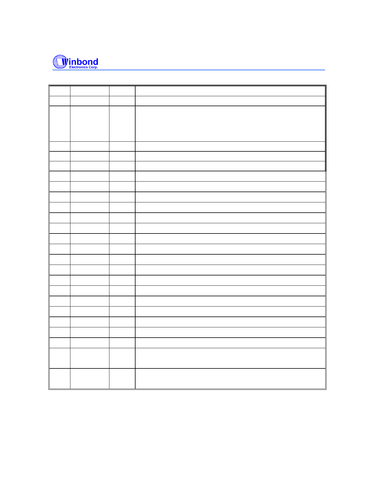
Pin Description, continued
NO.
PIN
9
BUSY
10 LED
11
VSSD
12
VSSA
13 SPK-
14 SPK+
15
VCCA
16 AUD
17
VCCA
18 OSC
19 MICREF
20 MIC
21 AGC
22
VCCD
23 CPU
24 SMODE
25 TEST
26 EXTCLK
27 RESET
28 L_REC
29 L_PLAY
30 E_PLAY
31 ERASE
32 FWD
I/O
DESCRIPTION
O Output busy signal, HIGH during playback
O Blink (Flash (volume-controlled) during playback
Flash Blink (3 Hz) when during low battery is low, segment full, or
memory full
ON during recording, erasing, and memory formatting
- Digital negative power supply
- Analog negative power supply
O Speaker voltage output -
O Speaker voltage output +
- Analog positive power supply
O Speaker current output (maximum 5 mA when VCC = 4.5V)
- Analog positive power supply +
I Oscillation frequency control pin
I Microphone reference
I Microphone input
I Automatic gain control input
- Digital positive power supply
I Normal/CPU mode select pin: low for normal, high for CPU
I Multi/single segment select pin: low for multi, high for single
I External test pin for testing
I External clock pin for testing
I Reset control pin
I Level record control pin
I Level playback control pin
I Edge playback control pin
I Message erase control pin in normal mode
Input level signal (from MCU) in CPU mode
I/O Message forward control pin in normal mode
Output level signal (to MCU) in CPU mode
Publication Release Date: April 1997
-3-
Revision A2
Share Link: 