CS8121 Просмотр технического описания (PDF) - Cherry semiconductor
Номер в каталоге
Компоненты Описание
Список матч
CS8121 Datasheet PDF : 8 Pages
| |||
Circuit Description: continued
If the input voltage rises above 30V (e.g. load dump), the
output shuts down. This response protects the internal cir-
cuitry and enables the IC to survive unexpected voltage
transients.
Using an emitter sense scheme, the amount of current
through the NPN pass transistor is monitored. Feedback
circuitry insures that the output current never exceeds a
preset limit.
Should the junction temperature of the power device
exceed 180ûC (typ) the power transistor is turned off.
Thermal shutdown is an effective means to prevent die
overheating since the power transistor is the principle
heat source in the IC.
Regulator Control Functions
The CS8121 contains two microprocessor compatible con-
trol functions: ENABLE and RESET (Figure 3).
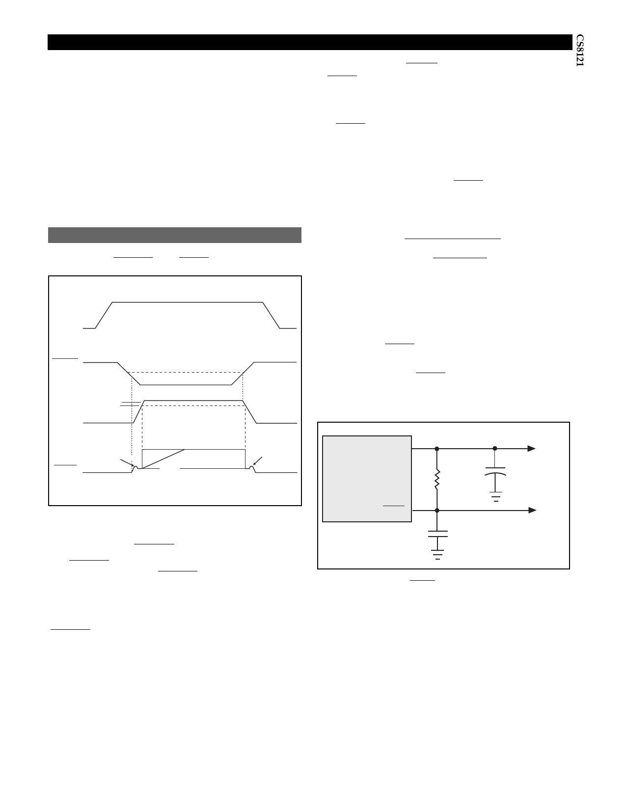
RESET Function
A RESET signal (low voltage) is generated as the IC pow-
ers up (VOUT > VOUT - 100mV) or when VOUT drops out of
regulation (VOUT < VOUT - 140mV, typ). 40mV of hysteresis
is included in the function to minimize oscillations.
The RESET output is an open collector NPN transistor,
controlled by a low voltage detection circuit. The circuit is
functionally independent of the rest of the IC, thereby
guaranteeing that the RESET signal is valid for VOUT as
low as 1V.
An external RC network on the RESET lead (Figure 4) pro-
vides a sufficiently long delay for most microprocessor
based applications. RC values can be chosen using the
following formula:
[ ( ) ] RTOT´CRST
ln
ÐtDelay
VT Ð VOUT
VRST Ð VOUT
VIN
ENABLE
VOUT
HI
VIN(HI)
LO
VRT(ON)
VRT(OFF)
FOR 7V < VIN < 26V
where:
RTOT = RRST in parallel with RIN,
RIN = µP port impedance,
CRST = RESET delay capacitor,
tDelay = desired delay time,
VRST = VSAT of RESET lead (0.7V @ turn - on), and
VT = µP logic threshold voltage.
RESET
VR PEAK
(1)
(2)
VR SAT
(1) = NO RESET DELAY CAPACITOR
(2) = WITH RESET DELAY CAPACITOR
Figure 3. Circuit Waveforms for the CS8121
VR PEAK
ENABLE Function
The ENABLE function switches the output transistor.
When the voltage on the ENABLE lead exceeds 2.9V typ,
the output pass transistor turns off, leaving a high
impedance facing the load. The IC will remain in Sleep
mode, drawing only 250µA, until the voltage on the lead
drops below 2.1V typ. Hysteresis (800mV) is built into the
ENABLE function to provide good noise immunity.
VOUT
CS8121
RESET
RRST
CRST
Figure 4. RC Network for RESET Delay
5V to mP
and
System
10mF Power
tantalum
to mP
RESET
Port
5
Share Link: 