CS5317 Просмотр технического описания (PDF) - Cirrus Logic
Номер в каталоге
Компоненты Описание
Список матч
CS5317 Datasheet PDF : 32 Pages
| |||
CS5317
Mode
Symbol
Mode
Pin
RESET
Output Word
Rate Provides
System-level 2X
Oversampling
CLKIN
(kHz)
Clock
Gen. 2
CLKG2 0V HIGH
CLKG2
CLKG2
NO
7.2
9.6
10.0 (max)
Clock
Gen. 1
CLKG1 +5V HIGH
CLKG1
CLKG1
YES
14.4
19.2
20.0 (max)
Clock
Override
CLKOR
CLKOR
CLKOR
-5V
SYNC
YES
3686.4
4915.2
5120.0 (max)
CS5316 CS5316 FSYNC LOW
YES
5120.0 (max)
* tdcD - Delay from CLKIN rising to DOUT falling = 1 CLKOUT cycle
CLKOUT
fsin
(MHz)
1.8432
2.4576
2.56
1.8432
2.4576
2.56
1.8432
2.4576
2.56
2.56
DOUT
fsout
(kHz)
7.2
9.6
10.0
14.4
19.2
20.0
14.4
19.2
20.0
20.0
F
(kHz)
14.4
19.2
20.0
14.4
19.2
20.0
14.4
19.2
20.0
20.0
tdcD*
(ns)
542.5
406.9
390.6
542.5
406.9
390.6
N/A
N/A
N/A
N/A
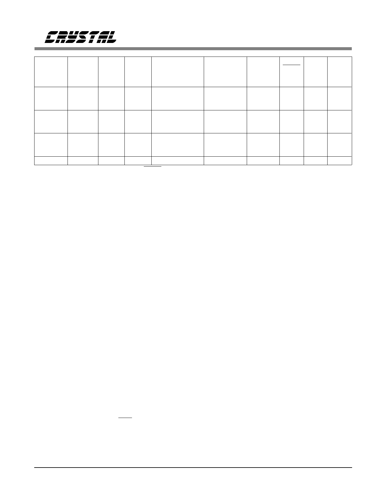
Table 1. Mode Comparisons
The second PLL mode is termed Clock Genera-
tion 2 (CLKG2) which generates its 5.12 MHz
clock from a 10 kHz external sampling signal.
Again, output samples are available at the system
sampling rate set by CLKIN, typically 10 kHz.
For the full-rated 10 kHz clock CLKG2 still sets
the filter’s 3 dB point at 5 kHz. Therefore,
CLKG2 provides no oversampling beyond the
Nyquist requirement at the system level
(10 kHz : 5 kHz) and its internal digital filter pro-
vides little anti-aliasing value. The CLKG2 mode
is initiated by grounding the MODE pin.
The CS5317 features a third operating mode
called Clock Override (CLKOR). Initiated by ty-
ing the MODE pin to -5V, CLKOR allows the
5.12 MHz master clock to be driven directly into
the CLKIN pin. The CS5317 then processes sam-
ples updating its output register at fclkin/256.
Since all clocking is generated internally, the
CLKOR mode includes a Reset capability which
allows the output samples of multiple CS5317’s
to be synchronized.
The CS5317 also has a CS5316 compatible
mode, selected by tying RST low, and using
MODE (pin 7) as the FSYNC pin. See the
CS5316 data sheet for detailed timing informa-
tion.
Analog Design Considerations
DC Characteristics
The CS5317 was designed for signal processing.
Its analog modulator uses CMOS amplifiers re-
sulting in offset and gain errors which drift over
temperature. If the CS5317 is being considered
for low-frequency (< 10 Hz) measurement appli-
cations, Crystal Semiconductor recommends the
CS5501, a low-cost, d.c. accurate, delta-sigma
ADC featuring excellent 60 Hz rejection and a
system-level calibration capability.
The Analog Input Range and Coding Format
The input range of the CS5317 is nominally ± 3V,
with ± 250 mV possible gain error. Because of
this gain error, analog input levels should be kept
below ± 2.75V. The converter’s serial output ap-
pears MSB-first in 2’s complement format.
Antialiasing Considerations
In applying the CS5317, aliasing occurs during
both the initial sampling of the analog input at fsin
(~2.5 MHz) and during the digital decimation
process to the 16-bit output sample rate, fsout.
8
DS27F4
Share Link: 