IDT74FCT273ATE Просмотр технического описания (PDF) - Integrated Device Technology
Номер в каталоге
Компоненты Описание
Список матч
IDT74FCT273ATE Datasheet PDF : 7 Pages
| |||
IDT54/74FCT273T/AT/CT FAST CMOS
OCTAL D FLIP-FLOP WITH MASTER RESET
MILITARY AND COMMERCIAL TEMPERATURE RANGES
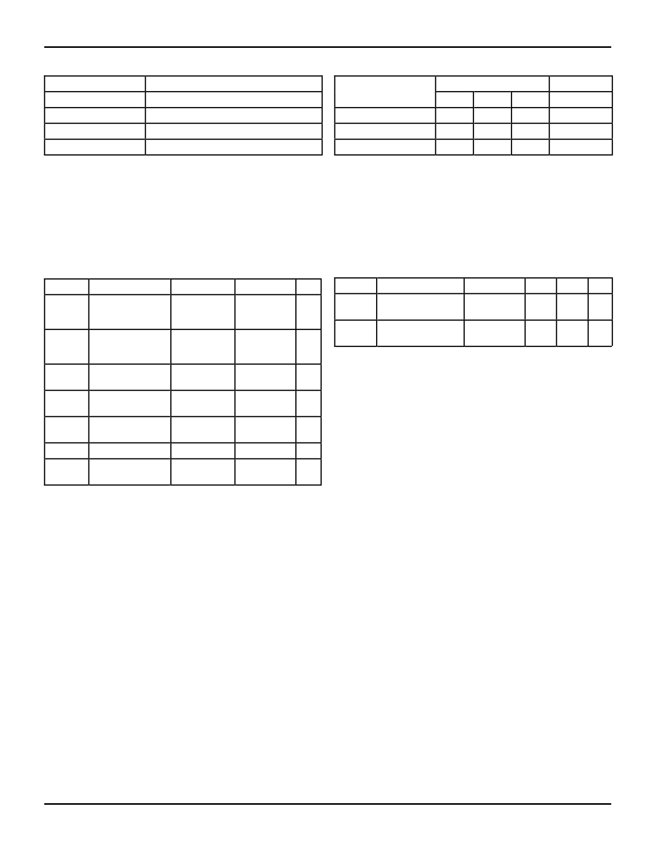
PIN DESCRIPTION
FUNCTION TABLE(1)
Pin Names
DN
MR
CP
ON
Description
Data Inputs
Master Reset (Active LOW)
Clock Pulse Input (Active Rising Edge)
Data Outputs
2568 tbl 01
Operating Mode
Inputs
MR
CP
DN
Outputs
ON
Reset (Clear)
L
X
X
L
Load "1"
H
↑
h
H
Load "0"
H
↑
I
L
NOTE:
2568 tbl 02
1. H = HIGH voltage level steady state
h = HIGH voltage level one set-up time prior to the LOW-to-HIGH clock
transition
L = LOW voltage level steady state
I = LOW voltage level one set-up time prior to the LOW-to-HIGH clock
transition
X = Don’t Care
↑ = LOW-to-HIGH Clock Transition
ABSOLUTE MAXIMUM RATINGS(1)
Symbol
Rating
VTERM(2) Terminal Voltage
with Respect to
GND
VTERM(3) Terminal Voltage
with Respect to
GND
TA
Operating
Temperature
TBIAS Temperature
Under Bias
TSTG Storage
Temperature
PT
Power Dissipation
Commercial
–0.5 to +7.0
–0.5 to
VCC +0.5
0 to +70
–55 to +125
–55 to +125
0.5
Military
–0.5 to +7.0
–0.5 to
VCC +0.5
–55 to +125
–65 to +135
–65 to +150
0.5
Unit
V
V
°C
°C
°C
W
IOUT
DC Output
–60 to +120 –60 to +120 mA
Current
NOTES:
2568 lnk 03
1. Stresses greater than those listed under ABSOLUTE MAXIMUM RAT-
INGS may cause permanent damage to the device. This is a stress rating
only and functional operation of the device at these or any other conditions
above those indicated in the operational sections of this specification is
not implied. Exposure to absolute maximum rating conditions for
extended periods may affect reliability. No terminal voltage may exceed
VCC by +0.5V unless otherwise noted.
2. Input and VCC terminals only.
3. Outputs and I/O terminals only.
CAPACITANCE (TA = +25°C, f = 1.0MHz)
Symbol Parameter(1) Conditions Typ. Max. Unit
CIN
Input
VIN = 0V
6
10 pF
Capacitance
COUT Output
VOUT = 0V 8
12 pF
Capacitance
NOTE:
2568 lnk 04
1. This parameter is measured at characterization but not tested.
6.10
2
Share Link: 