IDT74FCT162501AT(2009) Просмотр технического описания (PDF) - Integrated Device Technology
Номер в каталоге
Компоненты Описание
Список матч
IDT74FCT162501AT Datasheet PDF : 7 Pages
| |||
IDT74FCT162501AT/CT
FAST CMOS 18-BIT REGISTERED TRANSCEIVER
INDUSTRIAL TEMPERATURE RANGE
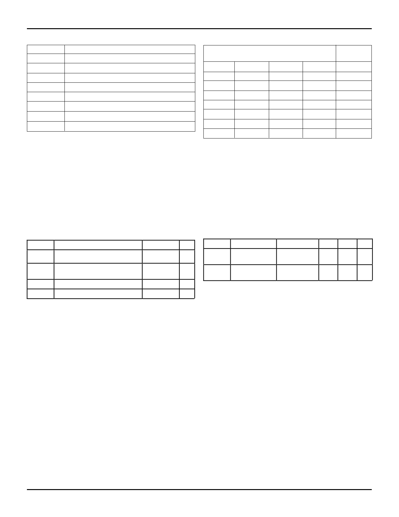
DC ELECTRICAL CHARACTERISTICS OVER OPERATING RANGE
Following Conditions Apply Unless Otherwise Specified:
Industrial: TA = –40°C to +85°C, VCC = 5.0V ±10%
Symbol
Parameter
Test Conditions(1)
Min. Typ.(2)
Max.
Unit
VIH
Input HIGH Level
Guaranteed Logic HIGH Level
2
—
—
V
VIL
Input LOW Level
Guaranteed Logic LOW Level
—
—
0.8
V
IIH
Input HIGH Current (Input pins)(5) VCC = Max.
VI = VCC
—
—
±1
µA
Input HIGH Current (I/O pins)(5)
—
—
±1
IIL
Input LOW Current (Input pins)(5)
VI = GND
—
—
±1
Input LOW Current (I/O pins)(5)
—
—
±1
IOZH
High Impedance Output Current VCC = Max.
VO = 2.7V
—
—
±1
µA
IOZL
(3-State Output pins)(5)
VO = 0.5V
—
—
±1
VIK
Clamp Diode Voltage
VCC = Min., IIN = –18mA
—
–0.7
–1.2
V
IOS
Short Circuit Current
VCC = Max., VO = GND(3)
–80
–140
–250
mA
VH
Input Hysteresis
—
ICCL
Quiescent Power Supply Current VCC = Max.
ICCH
VIN = GND or VCC
ICCZ
—
100
—
mV
—
5
500
µA
OUTPUT DRIVE CHARACTERISTICS
Symbol
IODL
IODH
Parameter
Output LOW Current
Output HIGH Current
Test Conditions(1)
VCC = 5V, VIN = VIH or VIL, VO = 1.5V(3)
VCC = 5V, VIN = VIH or VIL, VO = 1.5V(3)
Min. Typ.(2) Max. Unit
60
115
200 mA
–60
–115 –200 mA
VOH
Output HIGH Voltage
VCC = Min.
IOH = –24mA
2.4
3.3
—
V
VIN = VIH or VIL
VOL
Output LOW Voltage
VCC = Min.
IOL = 24mA
—
0.3
0.55
V
VIN = VIH or VIL
NOTES:
1. For conditions shown as Min. or Max., use appropriate value specified under Electrical Characteristics for the applicable device type.
2. Typical values are at VCC = 5.0V, +25°C ambient.
3. Not more than one output should be shorted at one time. Duration of the test should not exceed one second.
4. Duration of the condition can not exceed one second.
5. The test limit for this parameter is ±5µA at TA = –55°C.
3
Share Link: 