ADM4850ACP-REEL7 Просмотр технического описания (PDF) - Analog Devices
Номер в каталоге
Компоненты Описание
Список матч
ADM4850ACP-REEL7
Analog Devices

ADM4850ACP-REEL7 Datasheet PDF : 16 Pages
| |||
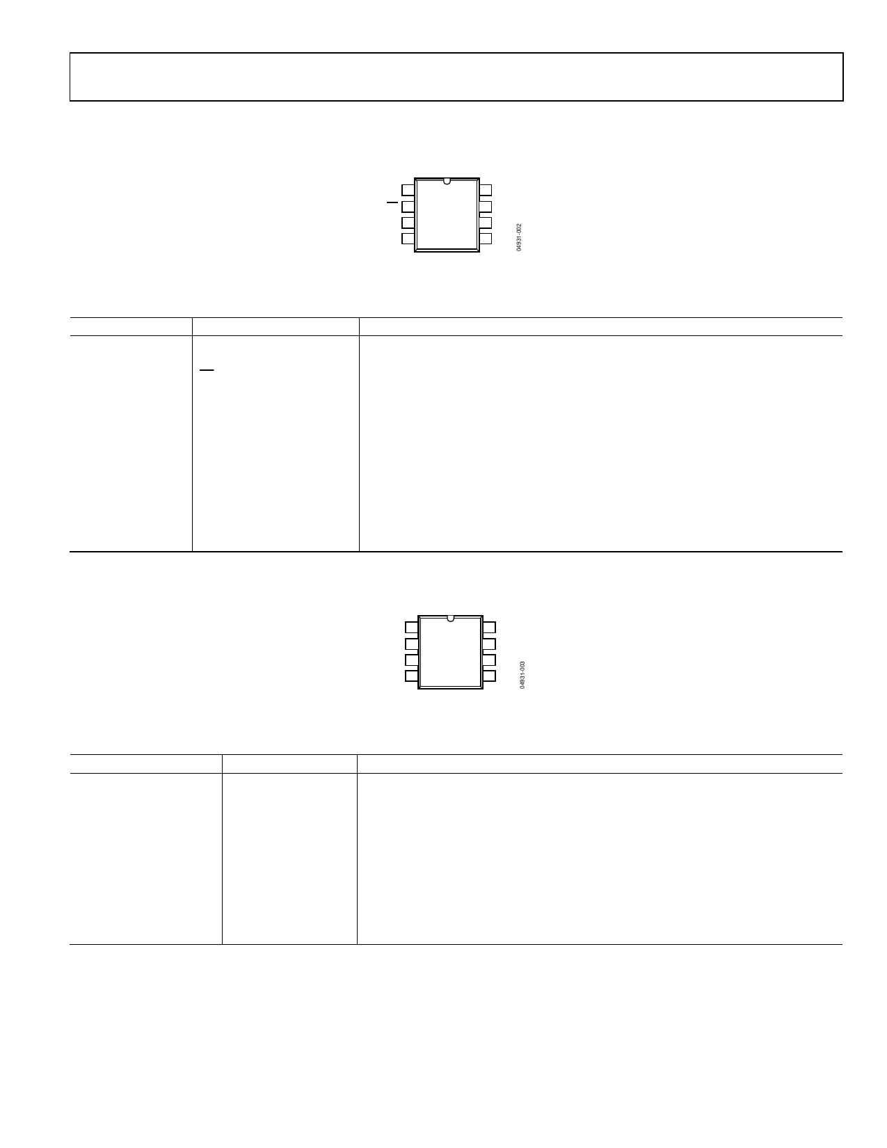
PIN CONFIGURATIONS AND FUNCTION DESCRIPTIONS
ADM4850–ADM4857
RO 1 ADM4850/ 8 VCC
ADM4851/
RE 2 ADM4852/ 7 B
DE 3 ADM4853 6 A
TOP VIEW
DI 4 (Not to Scale) 5 GND
Figure 2. ADM4850–ADM4853 Pin Configuration
Table 8. ADM4850–ADM4853 Pin Descriptions
Pin No.
Mnemonic
1
RO
2
RE
3
DE
4
DI
5
GND
6
A
7
B
8
VCC
Description
Receiver Output. When enabled, if (A−B) ≥ −30 mV, then RO = high.
If (A−B) ≤ −200 mV, then RO = low.
Receiver Output Enable.
A low level enables the receiver output, RO.
A high level places it in a high impedance state.
Driver Output Enable. A high level enables the driver differential inputs A and B.
A low level places it in a high impedance state.
Driver Input. When the driver is enabled, a logic low on DI forces A low and B high,
while a logic high on DI forces A high and B low.
Ground.
Noninverting Receiver Input A/Driver Output A.
Inverting Receiver Input B/Driver Output B.
5 V Power Supply.
VCC 1 ADM4854/ 8 A
RO
2
ADM4855/
ADM4856/
7
B
DI 3 ADM4857 6 Z
TOP VIEW
GND 4 (Not to Scale) 5 Y
Figure 3. ADM4854–ADM4857 Pin Configuration
Table 9. ADM4854–ADM4857 Pin Descriptions
Pin No.
Mnemonic
1
VCC
2
RO
3
DI
4
GND
5
Y
6
Z
7
B
8
A
Description
5 V Power Supply.
Receiver Output. When enabled, if (A−B) ≥ −30 mV, then RO = high.
If (A−B) ≤ −200 mV, then RO = low.
Driver Input. When the driver is enabled, a logic low on DI forces Y low and Z high,
while a logic high on DI forces Y high and Z low.
Ground.
Driver Noninverting Output.
Driver Inverting Output.
Receiver Inverting Input.
Receiver Noninverting Input.
Rev. 0 | Page 7 of 16
Share Link: