SP481E Просмотр технического описания (PDF) - Signal Processing Technologies
Номер в каталоге
Компоненты Описание
Список матч
SP481E Datasheet PDF : 11 Pages
| |||
RO 1
R
8 VCC
RE 2
7B
DE 3
6A
D
DI 4
SP485 5 GND
Top View
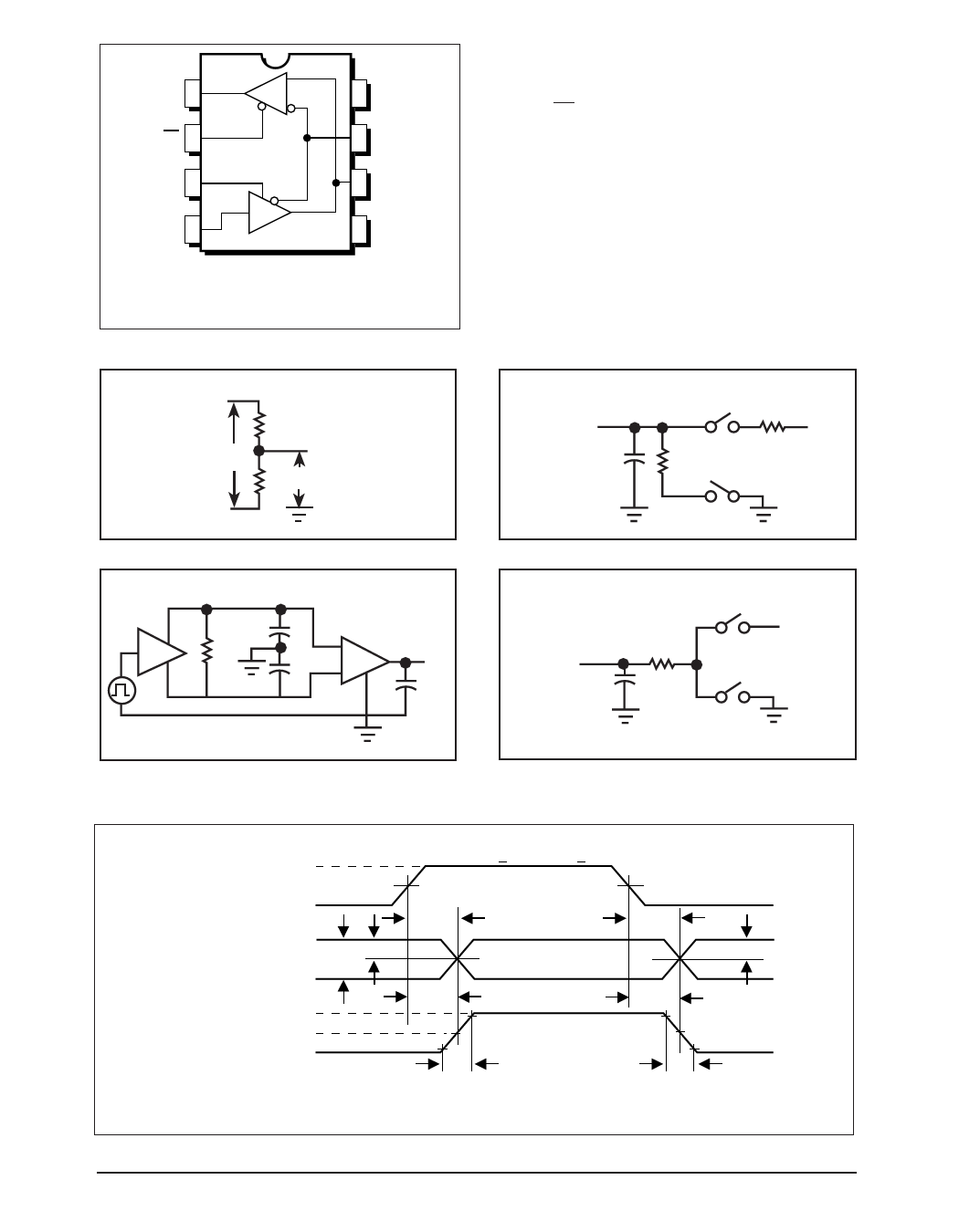
SP481E and SP485E
Pinout (Top View)
PIN FUNCTION
Pin 1 – RO – Receiver Output.
Pin 2 – RE – Receiver Output Enable Active LOW.
Pin 3 – DE – Driver Output Enable Active HIGH.
Pin 4 – DI – Driver Input.
Pin 5 – GND – Ground Connection.
Pin 6 – A – Driver Output/Receiver Input
Non-inverting.
Pin 7 – B – Driver Output/Receiver Input Inverting.
Pin 8 – Vcc – Positive Supply 4.75V<Vcc< 5.25V.
A
R
VOD
B
R VOC
Figure 1. RS-485 Driver DC Test Load Circuit
Receiver Test Point
Output
CRL
S1
1k
1k
VCC
S2
Figure 2. Receiver Timing Test Load Circuit
DI
A RDICFFL1
A
RO
B
B
CL2
15pF
Output
500
S1
VCC
Under
Test
CL
S2
Figure 3. RS-485 Driver/Receiver Timing Test Circuit Figure 4. RS-485 Driver Timing Test Load #2 Circuit
+3V
DI
0V
B
DRIVER
OUTPUT A
DIFFERENTIAL VO+
OUTPUT 0V
VA – VB VO–
tSKEW = | tDPLH - tDPHL |
f = 1MHz; tR < 10ns; tF < 10ns
1.5V
tPLH
tPHL
VO 1/2VO
tDPLH
tDPHL
tR
1.5V
1/2VO
tF
Figure 5. Driver Propagation Delays
Date: 02/24/05
SP481E Low Power Half-Duplex RS485 Transceivers
4
© Copyright 2005 Sipex Corporation
Share Link: 