74ACT16646 Просмотр технического описания (PDF) - Fairchild Semiconductor
Номер в каталоге
Компоненты Описание
Список матч
74ACT16646 Datasheet PDF : 6 Pages
| |||
Function Table
Inputs
Data I/O (Note 1)
G1
DIR1 CPAB1 CPBA1 SAB1 SBA1 A0–7
B0–7
Output Operation Mode
H
H
H
X
X
X
H or L
X
H or L
X
X
X
X
X
Isolation
X
Input Input Clock An Data into A Register
X
Clock Bn Data Into B Register
L
L
H
H
X
X
X
L
L
X
An to Bn—Real Time (Transparent Mode)
X
Input Output Clock An Data to A Register
L
L
H
H
H or L
X
X
H
H
X
X
A Register to Bn (Stored Mode)
Clock An Data into A Register and Output to Bn
L
L
L
L
X
X
X
X
X
L
Bn to An—Real Time (Transparent Mode)
L Output Input Clock Bn Data into B Register
L
L
L
L
H = HIGH Voltage Level
X
X
H or L
X
X
H
H
X = Immaterial L = LOW Voltage Level
B Register to An (Stored Mode)
Clock Bn into B Register and Output to An
= LOW-to-HIGH Transition.
Note 1: The data output functions may be enabled or disabled by various signals at the G and DIR inputs. Data input functions are always enabled; i.e., data
at the bus pins will be stored on every LOW-to-HIGH transition of the appropriate clock inputs. Also applies to data I/O (A and B: 8-15) and #2 control pins.
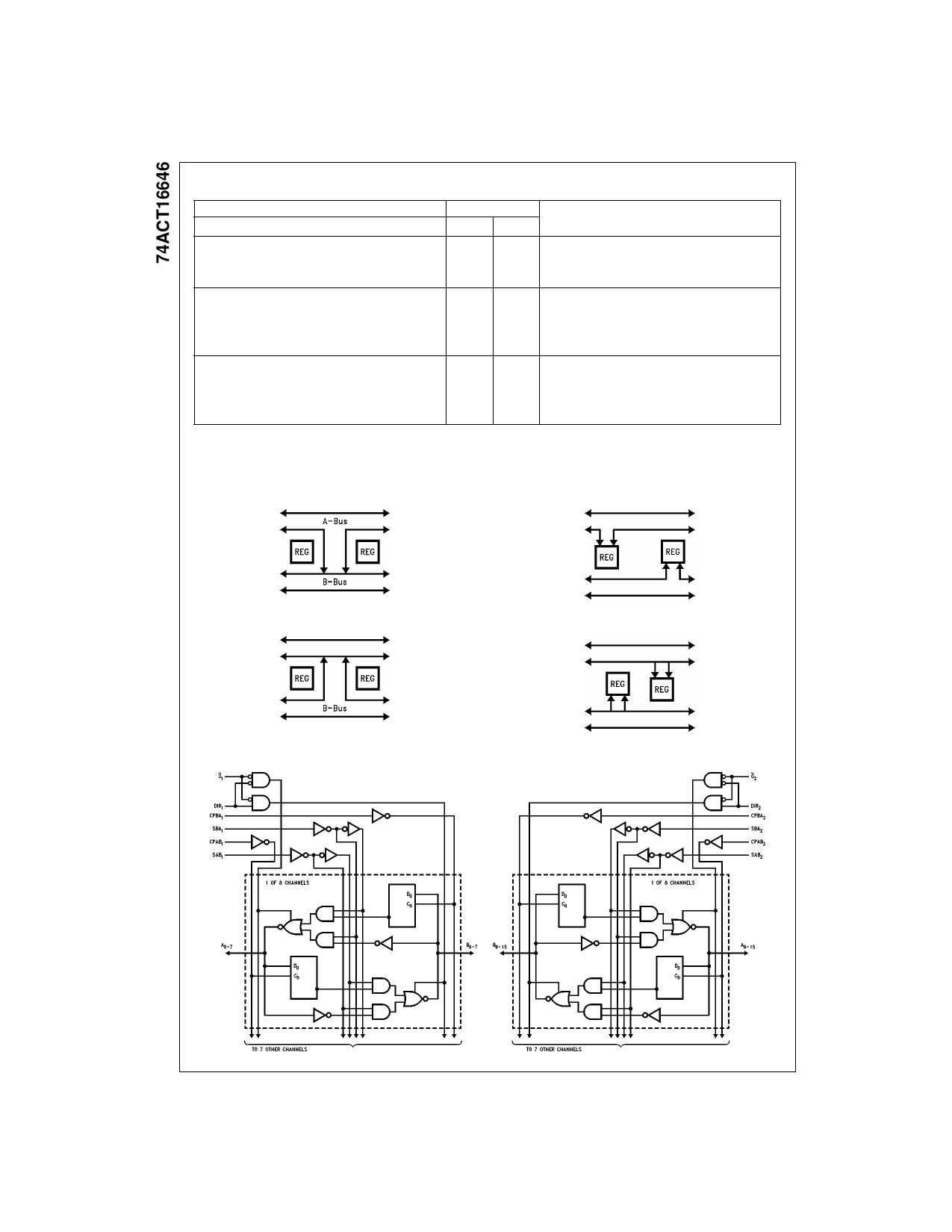
Real Time Transfer
A-Bus to B-Bus
Storage from
Bus to Register
Real Time Transfer
B-Bus to A-Bus
Transfer from
Register to Bus
Logic Diagram
www.fairchildsemi.com
2
Share Link: 