CS5471-BS Просмотр технического описания (PDF) - Cirrus Logic
Номер в каталоге
Компоненты Описание
Список матч
CS5471-BS Datasheet PDF : 14 Pages
| |||
CS5471
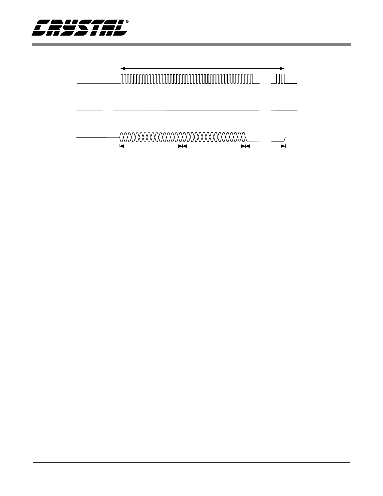
SCLK
96 SCLK Cycles
...
...
FSO
SDO
15 14 13 12 11 10 9 8 7 6 5 4 3 2 1 0 15 14 13 12 11 10 9 8 7 6 5 4 3 2 1 0
Channel 1 ( V )
Channel 1 ( I )
...
All 0’s
Figure 4. Close-up of One Frame
Data out (SDO) changes as a result of SCLK fall-
ing, and always outputs valid data with SCLK ris-
ing. When data is being transferred, the SCLK
frequency is either 1/8 of the XIN input frequency
(when OWRS is held low) or 1/4 of the XIN input
frequency (when OWRS is held high). Any other
time, SCLK is held low. (See Figures 3 and 4.)
The framing signal (FSO) output is normally low,
but produces a high level pulse lasting one SCLK
period when the instantaneous voltage/current data
samples are about to be transmitted out of the serial
interface (after each A/D conversion cycle). Note
that SCLK is not active during FSO high.
For 96 SCLK periods after FSO falls, SCLK is ac-
tive and SDO produces valid output. Six channels
of 16 bit data are output, MSB first. First, the volt-
age and current measurements are output (in that
order). This is followed by four more 16-bit words
of zero-value data. SCLK will then be held low un-
til the next sample period.
2.5 System Initialization
When power to the CS5471 is applied, the chip
must be held in a reset condition using the RESET
input.
A hardware reset is initiated when the RESET pin
is forced low with a minimum pulse width of 50 ns.
2.6 Analog Inputs
The analog inputs of the CS5471 are bipolar volt-
age inputs: One voltage channel input pair (VIN+
and VIN-) and current channel input pair (IIN+ and
IIN-). The CS5471 accommodates a full scale
range of ±40 mV or ±800 mV on the Current Chan-
nel and ±800 mV on the Voltage Channel.
2.7 Voltage Reference
The CS5471 is specified for operation with a
+1.2 V reference between the VREFIN and AGND
pins. The converter includes an internal 1.2 V ref-
erence (50 ppm/°C drift) that can be used by con-
necting the VREFOUT pin to the VREFIN pin of
the device. If higher accuracy/stability is required,
an external reference can be used.
2.8 Using the Charge Pump Drive Pin
The low, stable analog power consumption and su-
perior supply rejection of the CS5471 allow for the
use of a simple charge-pump negative supply gen-
erator. The use of a negative supply alleviates the
need for level shifting of the analog inputs. The
CPD pin and capacitor C1 provide the necessary
analog supply current as shown in Figure 5. The
Schottky diodes D1 and D2 are chosen for their low
forward voltages and high-speed capabilities. The
capacitor C2 provides the required charge storage
9
Share Link: 