HFA1205IP Просмотр технического описания (PDF) - Intersil
Номер в каталоге
Компоненты Описание
Список матч
HFA1205IP Datasheet PDF : 15 Pages
| |||
HFA1205
Absolute Maximum Ratings
Voltage Between V+ and V-. . . . . . . . . . . . . . . . . . . . . . . . . . . . 11V
DC Input Voltage . . . . . . . . . . . . . . . . . . . . . . . . . . . . . . . . VSUPPLY
Differential Input Voltage . . . . . . . . . . . . . . . . . . . . . . . . . . . . . . . 8V
Output Current (Note 2) . . . . . . . . . . . . . . . . . Short Circuit Protected
30mA Continuous
60mA ≤ 50% Duty Cycle
ESD Rating
Human Body Model (Per MIL-STD-883 Method 3015.7) . . . 600V
Thermal Information
Thermal Resistance (Typical, Note 1)
θJA (oC/W)
PDIP Package . . . . . . . . . . . . . . . . . . . . . . . . . . . . .
105
SOIC Package . . . . . . . . . . . . . . . . . . . . . . . . . . . . .
160
Maximum Junction Temperature (Plastic Package) . . . . . . . 150oC
Maximum Storage Temperature Range . . . . . . . . . -65oC to 150oC
Maximum Lead Temperature (Soldering 10s) . . . . . . . . . . . . 300oC
(SOIC - Lead Tips Only)
Operating Conditions
Temperature Range. . . . . . . . . . . . . . . . . . . . . . . . . . -40oC to 85oC
CAUTION: Stresses above those listed in “Absolute Maximum Ratings” may cause permanent damage to the device. This is a stress only rating and operation of the
device at these or any other conditions above those indicated in the operational sections of this specification is not implied.
NOTES:
1. θJA is measured with the component mounted on a low effective thermal conductivity test board in free air. See Tech Brief TB379 for details.
2. Output is short circuit protected to ground. Brief short circuits to ground will not degrade reliability, however continuous (100% duty cycle) output
current must not exceed 30mA for maximum reliability.
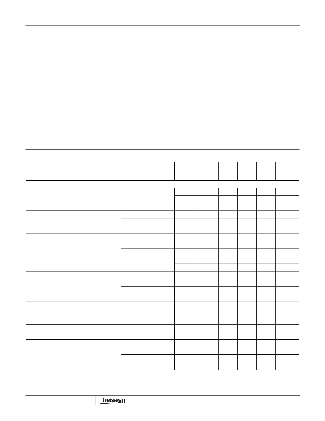
Electrical Specifications VSUPPLY = ±5V, AV = +1, RF = 560Ω, RL = 100Ω, Unless Otherwise Specified
PARAMETER
(NOTE 3)
TEST CONDITIONS
TEST TEMP.
LEVEL
(oC)
MIN
TYP
INPUT CHARACTERISTICS
Input Offset Voltage
A
25
-
2
A
Full
-
3
Average Input Offset Voltage Drift
B
Full
-
1
Input Offset Voltage
Common-Mode Rejection Ratio
Input Offset Voltage
Power Supply Rejection Ratio
Non-Inverting Input Bias Current
∆VCM = ±1.8V
∆VCM = ±1.8V
∆VCM = ±1.2V
∆VPS = ±1.8V
∆VPS = ±1.8V
∆VPS = ±1.2V
A
25
45
48
A
85
43
46
A
-40
43
46
A
25
48
52
A
85
46
50
A
-40
46
50
A
25
-
6
A
Full
-
10
Non-Inverting Input Bias Current Drift
B
Full
-
5
Non-Inverting Input Bias Current
Power Supply Sensitivity
Non-Inverting Input Resistance
Inverting Input Bias Current
∆VPS = ±1.8V
∆VPS = ±1.8V
∆VPS = ±1.2V
∆VCM = ±1.8V
∆VCM = ±1.8V
∆VCM = ±1.2V
A
25
-
0.5
A
85
-
0.8
A
-40
-
0.8
A
25
0.8
2
A
85
0.5
1.3
A
-40
0.5
1.3
A
25
-
2
A
Full
-
5
Inverting Input Bias Current Drift
B
Full
-
60
Inverting Input Bias Current
Common-Mode Sensitivity
∆VCM = ±1.8V
∆VCM = ±1.8V
∆VCM = ±1.2V
A
25
-
3
A
85
-
4
A
-40
-
4
MAX
5
8
10
-
-
-
-
-
-
15
25
60
1
3
3
-
-
-
8.5
15
200
6
8
8
UNITS
mV
mV
µV/ oC
dB
dB
dB
dB
dB
dB
µA
µA
nA / oC
µA / V
µA / V
µA / V
MΩ
MΩ
MΩ
µA
µA
nA / oC
µA / V
µA/ V
µA / V
2
Share Link: 