MX641DW Просмотр технического описания (PDF) - MX-COM Inc
Номер в каталоге
Компоненты Описание
Список матч
MX641DW Datasheet PDF : 16 Pages
| |||
Dual SPM Detector
11
MX641 PRELIMINARY INFORMATION
4.3.2 Fixed Sensitivity Setting
In this mode the sensitivity of each channel is set by the correct selection of the components around the Channel Input
Amplifier. Note that the device sensitivity is directly proportional to the applied power supply (VDD) and that the gain
bandwidth product of the input opamp can attenuate the SPM signal gain at some input gain configurations.
4.3.2.1 Input Gain Calculation
The input amplifier, with external circuitry, is used to set the sensitivity of the MX641 to conform to the user's national level
specification with regard to ‘Must’ and ‘Must-Not’ decode signal levels.
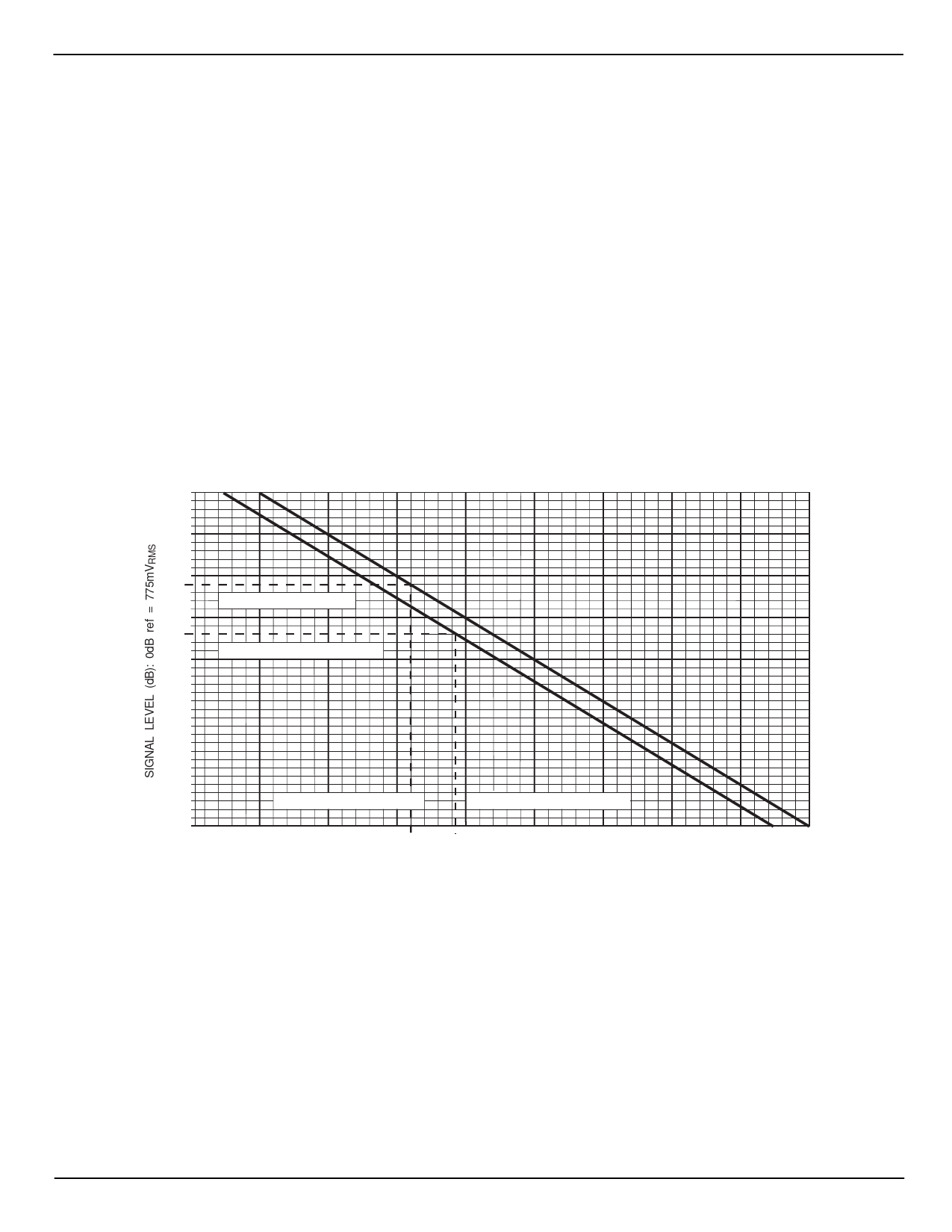
With reference to the graph in Figure 7, the following steps will assist in the determination of the required gain/attenuation.
Step 1
Step 2
Step 3
Draw two horizontal lines from the Y-axis (Signal Level) in Figure 7. The upper line represents the required
‘Must’ decode level. The lower line represents the required ‘Must-Not’ decode level
Mark the intersection of the upper horizontal line and the upper sloping line; drop a vertical line from this point to
the X-axis (Amplifier Gain (dB)). The point where the vertical line meets the X-axis indicates the minimum Input
Amp gain required for reliable decoding of valid signals
Mark the intersection of the lower horizontal line and the lower sloping line; drop a vertical line from this point to
the X-axis. The point where the vertical line meets the X-axis will indicate the maximum allowable Input Amp
gain. Input signals at or below the ‘Must-Not’ decode level will not be detected as long as the amplifier gain is
no higher than this level.
-10
-15
-20
MUST DECODE LEVEL
-25
MUST-NOT DECODE LEVEL
-30
-35
-40
-45
MINIMUM AMPLIFIER GAIN
MAXIMUM AMPLIFIER GAIN
-50
-20
-15
-10
-5
0
5
10
15
20
25
AMPLIFIER GAIN (dB)
VDD = 5.0 (±0.1) VOLTS; TEMP = -40°C to 85°C
Figure 7: Input Gain Calculation Graph for use in the Fixed Sensitivity Mode
4.3.2.2 Input Gain Components
Refer to the gain components shown in Figure 2. The user should calculate and select external components (R1/R3/C3,
R2/R4/C4 and R5/R7/C5, R6/R8/C6) to provide amplifier gains within the limits obtained in Steps 2 and 3.
Component tolerances should not move the gain-figure outside these limits. The graph in Figure 7 is for the calculation of
input gain components for an MX641 using a VDD of 5.0 (±0.1) volts.
It is recommended that the designed gain is near the center of the calculated range.
© 1998 MXxCOM Inc.
www.mxcom.com Tele: 800 638-5577 910 744-5050 Fax: 910 744-5054
Doc. # 20480115.003
4800 Bethania Station Road, Winston-Salem, NC 27105-1201 USA
All trademarks and service marks are held by their respective companies.
Share Link: 