74AC253PC Просмотр технического описания (PDF) - Fairchild Semiconductor
Номер в каталоге
Компоненты Описание
Список матч
74AC253PC Datasheet PDF : 8 Pages
| |||
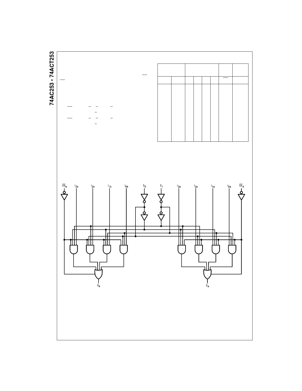
Functional Description
The AC/ACT253 contains two identical 4-input multiplexers
with 3-STATE outputs. They select two bits from four
sources selected by common Select inputs (S0, S1). The 4-
input multiplexers have individual Output Enable (OEa,
OEb) inputs which, when HIGH, force the outputs to a high
impedance (High Z) state. This device is the logic imple-
mentation of a 2-pole, 4-position switch, where the position
of the switch is determined by the logic levels supplied to
the two select inputs. The logic equations for the outputs
are shown:
Za = OEa • (I0a • S1 • S0 + I1a • S1 • S0 +
I2a • S1 • S0 + I3a • S1 • S0)
Zb = OEb • (I0b • S1 • S0 + I1b • S1 • S0 +
I2b • S1 • S0 + I3b • S1 • S0)
If the outputs of 3-STATE devices are tied together, all but
one device must be in the high impedance state to avoid
high currents that would exceed the maximum ratings.
Designers should ensure that Output Enable signals to 3-
STATE devices whose outputs are tied together are
designed so that there is no overlap.
Truth Table
Select
Inputs
Data Inputs
Output
Outputs
Enable
S0
S1
I0 I1 I2 I3
OE
Z
X
X XXXX H
Z
L
L
LXXX
L
L
L
L
HXXX
L
H
H
L
XLXX
L
L
H
L
XHXX
L
H
L
H
XX L X
L
L
L
H
XXHX
L
H
H
H
XXXL
L
L
H
H
XXXH
L
H
Address Inputs S0 and S1 are common to both sections.
H = HIGH Voltage Level
L = LOW Voltage Level
X = Immaterial
Z = High Impedance
Logic Diagram
Please note that this diagram is provided only for the understanding of logic operations and should not be used to estimate propagation delays.
www.fairchildsemi.com
2
Share Link: 