W48S87-72X Просмотр технического описания (PDF) - Cypress Semiconductor
Номер в каталоге
Компоненты Описание
Список матч
W48S87-72X Datasheet PDF : 19 Pages
| |||
W48S87-72
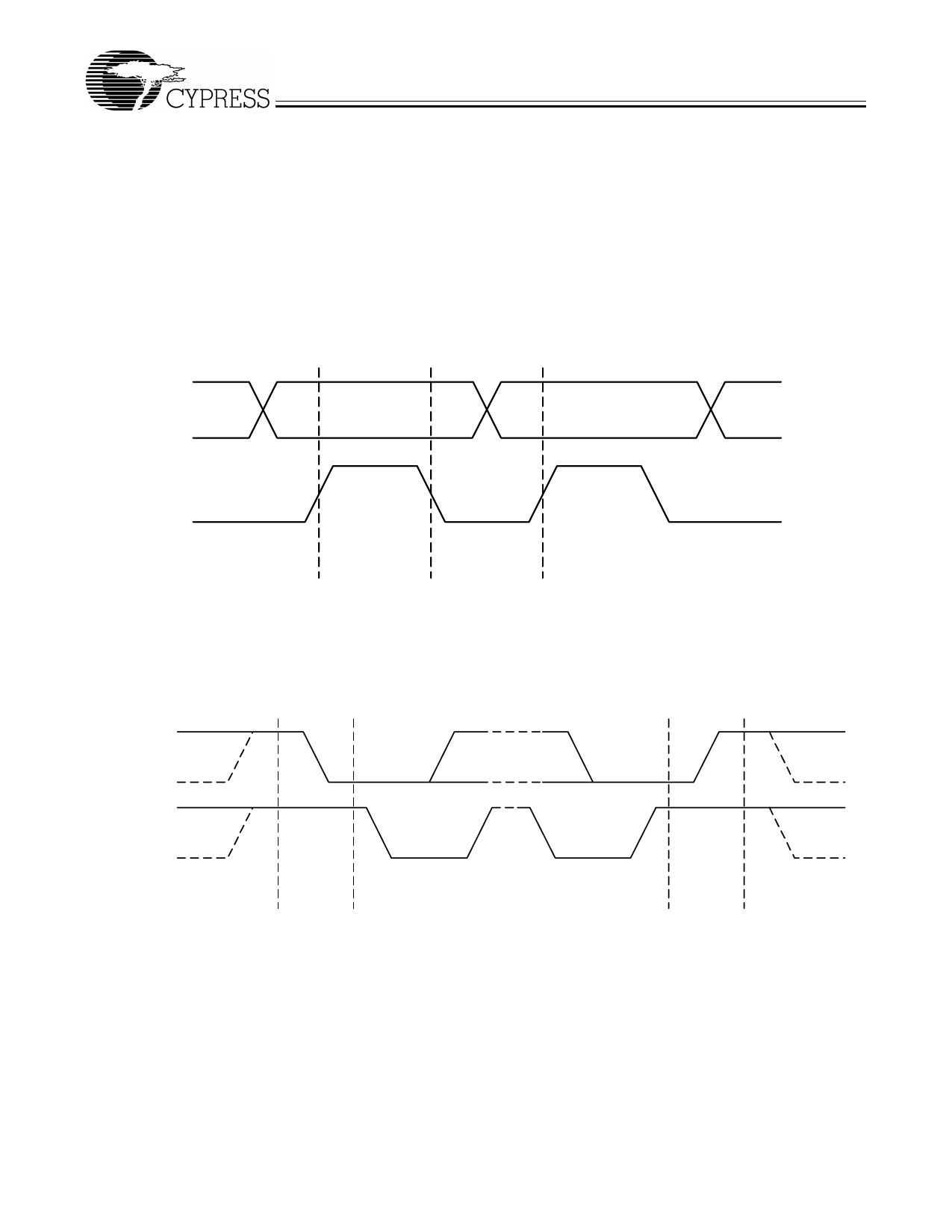
Signaling Requirements
As shown in Figure 4, valid data bits are defined as stable logic
0 or 1 condition on the data line during a clock HIGH (logic 1)
pulse. A transitioning data line during a clock HIGH pulse may
be interpreted as a start or stop pulse (it will be interpreted as
a start or stop pulse if the start/stop timing parameters are
met).
A write sequence is initiated by a “start bit” as shown in Figure
5. A “stop bit” signifies that a transmission has ended.
As stated previously, the W48S87-72 sends an “acknowledge”
pulse after receiving eight data bits in each byte as shown in
Figure 6.
Sending Data to the W48S87-72
The device accepts data once it has detected a valid start bit
and address byte sequence. Device functionality is changed
upon the receipt of each data bit (registers are not double buff-
ered). Partial transmission is allowed meaning that a transmis-
sion can be truncated as soon as the desired data bits are
transmitted (remaining registers will be unmodified). Transmis-
sion is truncated with either a stop bit or new start bit (restart
condition).
6'$7$
6&/2&.
9DOLG
'DWD
%LW
&KDQJH
RI 'DWD $OORZHG
Figure 4. Serial Data Bus Valid Data Bit
6'$7$
6&/2&.
6WDUW
6WRS
%LW
%LW
Figure 5. Serial Data Bus Start and Stop Bit
10
Share Link: 