W48S87(1999) Просмотр технического описания (PDF) - Cypress Semiconductor
Номер в каталоге
Компоненты Описание
Список матч
W48S87 Datasheet PDF : 21 Pages
| |||
PRELIMINARY
W48S87-04
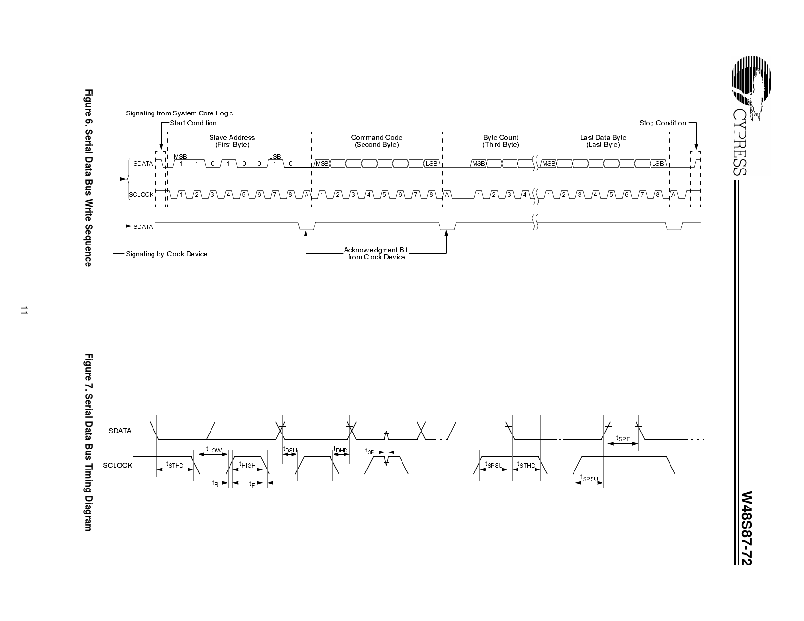
How To Use the Serial Data Interface
Electrical Requirements
Figure 5 illustrates electrical characteristics for the serial inter-
face bus used with the W48S87-04. Devices send data over
the bus with an open drain logic output that can (a) pull the bus
line LOW, or (b) let the bus default to logic 1. The pull-up resis-
tors on the bus (both clock and data lines) establish a default
logic 1. All bus devices generally have logic inputs to receive
data.
Although the W48S87-04 is a receive-only device (no data
write-back capability), it does transmit an “acknowledge” data
pulse after each byte is received. Thus, the SDATA line can
both transmit and receive data.
The pull-up resistor should be sized to meet the rise and fall
times specified in AC parameters, taking into consideration to-
tal bus line capacitance.
VDD
VDD
SERIAL BUS DATA LINE
SERIAL BUS CLOCK LINE
CLOCK IN
CLOCK OUT
SDCLK
DATA IN
N DATA OUT
~ 2kΩ
~ 2kΩ
SDATA
N
CLOCK IN
SCLOCK
DATA IN
DATA OUT
SDATA
N
CHIP SET
(SERIAL BUS MASTER TRANSMITTER)
CLOCK DEVICE
(SERIAL BUS SLAVE RECEIVER)
Figure 5. Serial Interface Bus Electrical Characteristics
11
Share Link: 