W921C880 Просмотр технического описания (PDF) - Winbond
Номер в каталоге
Компоненты Описание
Список матч
W921C880 Datasheet PDF : 57 Pages
| |||
W921E880A/W921C880
* P5.0−P5.3:
Multi-function I/O pins.
Normal function is the same as port P0
Special function
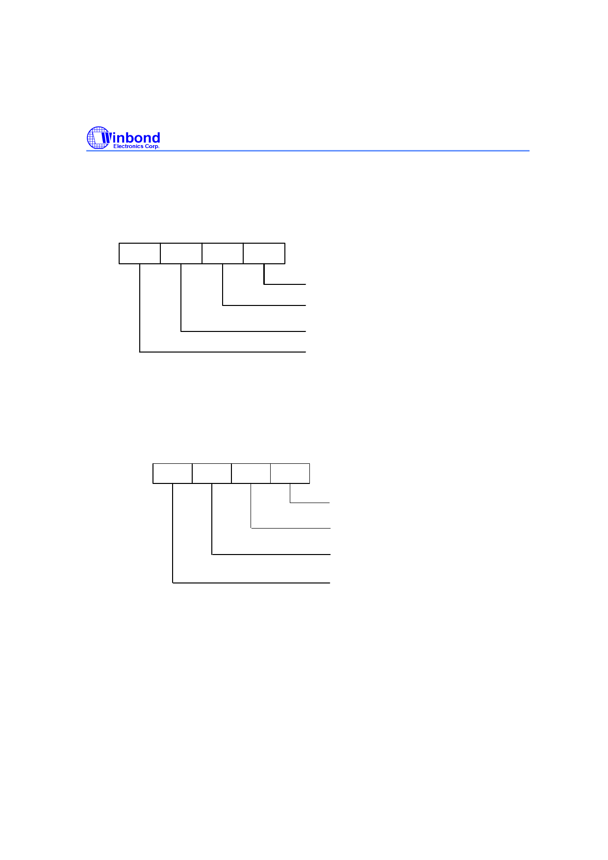
P5IO REG: (ADDRESS = 011H)
(Default data = 0H)
b3
b2
b1
b0
0: Normal I/O P5.0
1: Work as the timer 1 control pin
0: Normal I/O P5.1
1: Work as the timer 2 control pin
0: Normal I/O P5.2
1: Work as the Vref input pin of the comparator
0: Normal I/O P5.3
1: Work as the output pin of D/A converter
(DAOUT)
* P6.0−P6.3 :
Multi-function I/O pins.
Normal function is the same as port P0
Special function
P6IO REG: (ADDRESS = 012H)
(Default data = 0H)
b3
b2
b1
b0
0: Normal I/O P6.0
1: Work as the data output pin of the WCLK pin
(WDATA)
0: Normal I/O P6.1
1: Work as the clock I/O pin of the WDATA pin
(WCLK)
0: Normal I/O P6.2
1: Work as the data input pin of the RCLK pin
(RDATA)
0: Normal I/O P6.3
1: Work as the clock I/O pin of the RDATA pin
(RCLK)
* P8.0−P8.3 :
Four 10 mA drive current pins
Normal I/O pins only.
Normal function is the same as port P0
* P9.0−P9.3 :
Four 15 mA sink current pins
Normal I/O pins only.
Normal function is the same as port P0
* PA.0−PA.3 : Normal I/O pins only.
Normal function is the same as port P0
* PB.0−PB.3 : Normal I/O pins only.
- 16 -
Share Link: 