W567S010 Просмотр технического описания (PDF) - Winbond
Номер в каталоге
Компоненты Описание
Список матч
W567S010 Datasheet PDF : 13 Pages
| |||
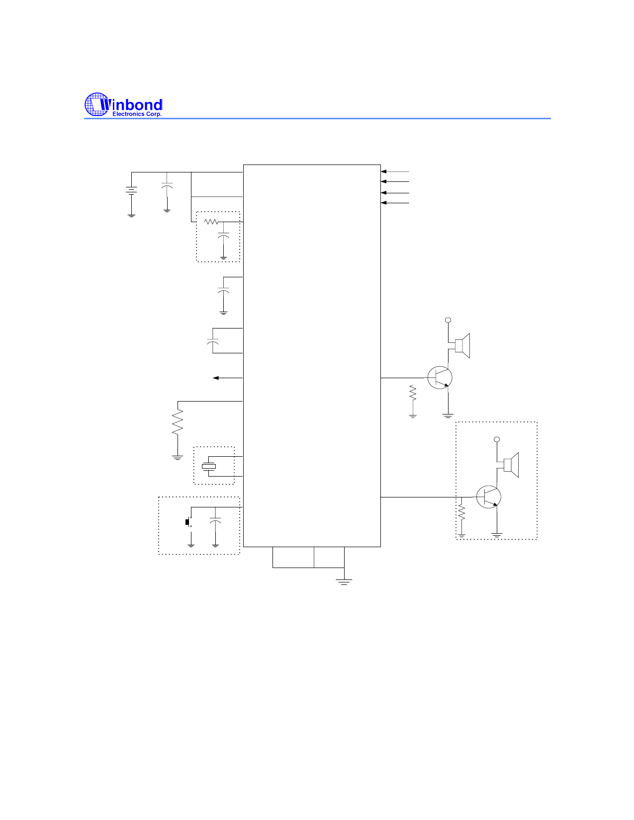
6.4 W567S301/S341 with ADC Application
+
Battery
4.7uF
10
0.1uF
22uF
C
ROSC
VDD
VDDA
VDDOSC
AVDD
CIN
COUT
VRB
OSC
W567S301
|
W567S341
IP00
IP01
IP02
IP03
IP04
|
IP07
BP00
|
BP07
BP10
|
BP17
BP20
|
BP27
DAC0
Reset
Switch
X32I
32K
X32O
/RESET
0.1uF
DAC1
VSSOSC VSSA VSS
W567SXXX
VDD
Speaker0
8050
VDD
Speaker1
8050
Notes:
1.
2.
3.
4.
5.
6.
7.
The typical value of Rosc is 150 KΩ for 8MHz and 300 KΩ for 4MHz and should be connected to GND (VSS).
Please refer to design guide to get typical Rosc value for each part number.
For W567S301~S341, VSSA and VSSOSC should be connected to VSS; and VDDA and VDDOSC should be
connected to VDD in PCB layout.
The Rs value is suggested in 270Ω ~ 1KΩ to limit too large DAC output current flowing into transistor.
The 10Ω and 0.1µF between VDD, VDDOSC and GND are optional to filter power noise.
The capacitor, 4.7µF, shunts between VDD and GND is necessary as power stability. But the value of capacitor is
depend on the application.
The above application circuits are for reference only. No warranty for mass production.
- 11 -
Publication Release Date: June 15, 2004
Revision A11
Share Link: 