EVB3011 Просмотр технического описания (PDF) - Agere -> LSI Corporation
Номер в каталоге
Компоненты Описание
Список матч
EVB3011 Datasheet PDF : 12 Pages
| |||
Data Sheet
September 1999
W3011
1 GHz Quadrature Modulator
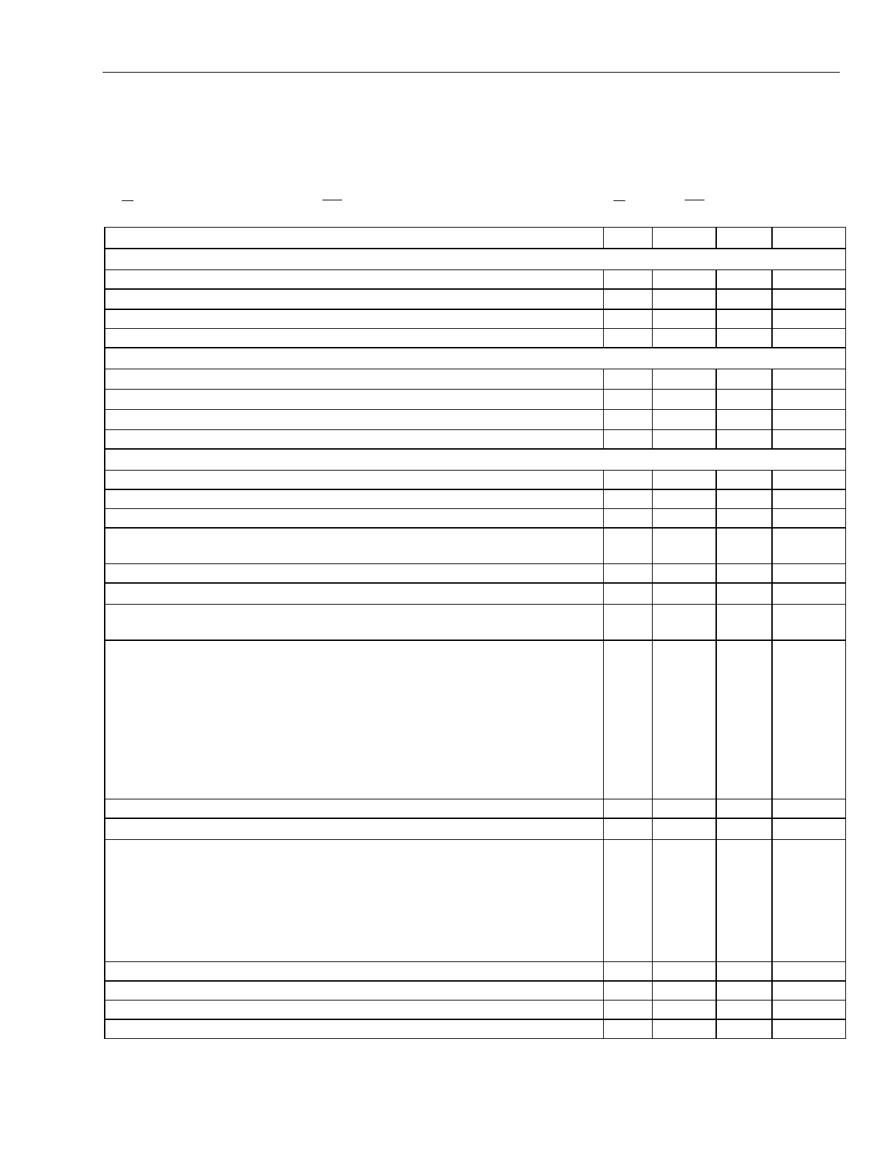
Electrical Characteristics (continued)
Table 5. ac Specifications
Conditions unless otherwise noted: 2.7 ≤ VCC ≤ 3.3 Vdc; TA = 25 °C ± 3 °C; RL = 50 Ω, VAPC = 2.7 Vdc;
fRF = 900 MHz, fLOL = 130 MHz, fLOH = 1030 MHz, –15 dBm < PLOL, PLOH < –5 dBm;
I – I = 0.4 cos(2πt Ÿ 80 kHz), Q – Q = 0.4 cos(2πt Ÿ 80 kHz – π/2), Vbias of I, I , Q, and Q = 1.22 Vdc.
Parameter
Min Typ Max Unit
I&Q
I & Q Signal Path 0.5 dB Bandwidth
—
5
—
MHz
I & Q Input Resistance
— 200
—
kΩ
I & Q Input Capacitance to Ground
—
5
—
pF
I & Q Input Differential Signal for Max Output
—
0.8
—
Vp-p
Offset Mixer
LOL Input Impedance
LOH Input Impedance
—
50
—
Ω
—
50
—
Ω
LO Input Impedance (pins LC1, LC2)
— 480//1 —
Ω//pF
LOL Input IP3
—
10
—
dBm
Modulation Accuracy (POUT = –1 dBm)
Carrier Suppression (POUT = –1 dBm)
— –35 –28 dBUSB
Carrier Suppression (entire usable APC range)
—
—
–26 dBUSB
Origin Offset (DQPSK inputs, all usable APC levels)
—
—
–23
dBc
Error Vector Magnitude (See Explanation of Error Vector Magnitude
(EVM) Testing section.)
—
2.5
5
%
Lower Sideband (LSB) Suppression (See Figure 3.)
— –43 –34 dBUSB
RF Output
Output Power (0.8 Vp-p differential or single-ended 80 kHz sine-wave
inputs to I and Q, with 90° between I and Q)
–1
3
—
dBm
Adjacent Channel Suppression (0.282 Vrms differential I and Q inputs,
π/4 – DQPSK modulation, random data):
Per PDC (RCR STD-27):
±50 kHz, All Usable APC Levels
±100 kHz, All Usable APC Levels
±100 kHz, Max RF Output (APC > 2.2)
Per IS-136/IS-137 800 MHz Digital Mode:
±30 kHz, All Usable APC Levels
±60 kHz, All Usable APC Levels
— –65 –55
dBc
—
—
–62
dBc
— –75 –65
dBc
— –45 –36
dBc
— –60 –50
dBc
Noise Floor Suppression, FC ± >100 kHz
— –120 –112 dBc/Hz
APC (Automatic Power Control) Function
Range of Usable Output Power Control for Japan PDC (RCR STD-27),
from Max Power at APC = 2.7 V to Minimum APC Voltage Where
Requirements for ACP and Carrier Suppression Are Still Met Using
π/4 – DQPSK/α = 0.5 Modulation at 0.282 Vrms Differential I and Q
Inputs:
Offset Mixer Not Used
Offset Mixer Used
29
40
—
dB
39
45
—
dB
Output Power Variation Due to Temperature, within Usable Control Range —
4
6
dB
RF Power Change Time (after APC change)
—
—
2
µs
APC Voltage for Max Output Power
—
2.2
—
Vdc
APC Voltage for Min Output Power
—
0.8
—
Vdc
Lucent Technologies Inc.
5
Share Link: 