25X32BVFIG Просмотр технического описания (PDF) - Winbond
Номер в каталоге
Компоненты Описание
Список матч
25X32BVFIG Datasheet PDF : 45 Pages
| |||
W25X32BV
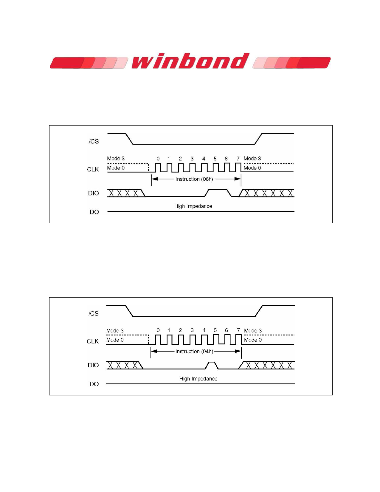
10.2.3 Write Enable (06h)
The Write Enable instruction (Figure 4) sets the Write Enable Latch (WEL) bit in the Status Register to
a 1. The WEL bit must be set prior to every Page Program, Sector Erase, Block Erase, Chip Erase
and Write Status Register instruction. The Write Enable instruction is entered by driving /CS low,
shifting the instruction code “06h” into the Data Input (DI) pin on the rising edge of CLK, and then
driving /CS high.
Figure 4. Write Enable Instruction Sequence Diagram
10.2.4 Write Disable (04h)
The Write Disable instruction (Figure 5) resets the Write Enable Latch (WEL) bit in the Status Register
to a 0. The Write Disable instruction is entered by driving /CS low, shifting the instruction code “04h”
into the DIO pin and then driving /CS high. Note that the WEL bit is automatically reset after Power-up
and upon completion of the Write Status Register, Page Program, Sector Erase, Block Erase and
Chip Erase instructions.
Figure 5. Write Disable Instruction Sequence Diagram
- 15 -
Publication Release Date: October 7, 2009
Preliminary -- Revision C
Share Link: 