W163 Просмотр технического описания (PDF) - Cypress Semiconductor
Номер в каталоге
Компоненты Описание
Список матч
W163 Datasheet PDF : 5 Pages
| |||
W163
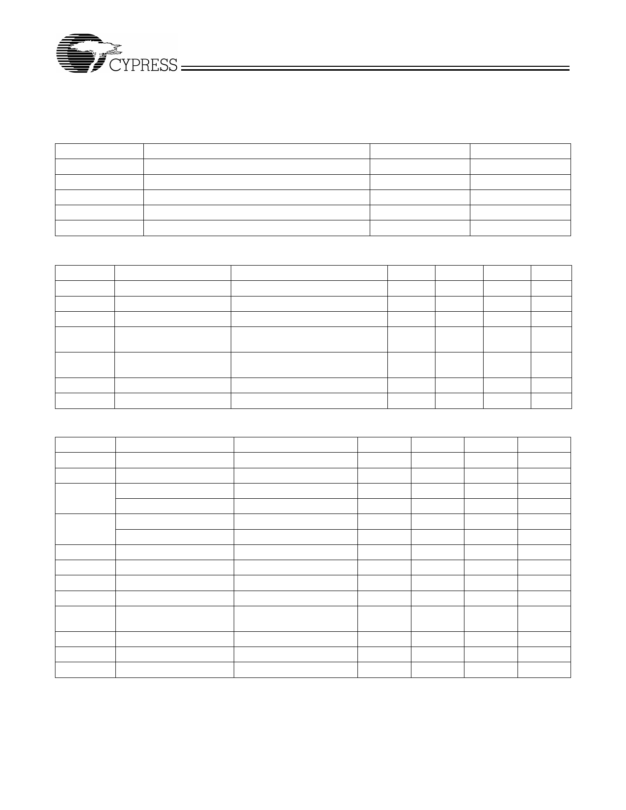
Absolute Maximum Ratings[1]
Stresses greater than those listed in this table may cause per-
manent damage to the device. These represent a stress rating
only. Operation of the device at these or any other conditions
.
Parameter
Description
VDD, VIN
TSTG
TA
TB
PD
Voltage on any pin with respect to GND
Storage Temperature
Operating Temperature
Ambient Temperature under Bias
Power Dissipation
above those specified in the operating sections of this specifi-
cation is not implied. Maximum conditions for extended peri-
ods may affect reliability.
Rating
Unit
–0.5 to +7.0
V
–65 to +150
°C
0 to +70
°C
–55 to +125
°C
0.5
W
DC Electrical Characteristics: TA =0°C to 70°C, VDD = 3.3V ±10%
Parameter
IDD
VIL
VIH
VOL
Description
Supply Current
Input Low Voltage
Input High Voltage
Output Low Voltage
VOH
Output High Voltage
IIL
Input Low Current
IIH
Input High Current
Test Condition
Unloaded, 100 MHz
IOL = 12 mA (-15)
IOL = 8 mA (-5)
IOL = 12 mA (-15)
IOL = 8 mA (-5)
VIN = 0V
VIN = VDD
Min
Typ
Max
Unit
40
mA
0.8
V
2.0
V
0.4
V
2.4
V
50
µA
100
µA
AC Electrical Characteristics: TA = 0°C to +70°C, VDD = 3.3V ±10%
Parameter
Description
Test Condition
Min
Typ
Max
Unit
fIN
Input Frequency
10
fOUT
Output Frequency
15-pF load[6]
10
tR
Output Rise Time (-05)[2] 2.0 to 0.8V, 15-pF load
Output Rise Time (-15)[2] 2.0 to 0.8V, 20-pF load
133
MHz
133
MHz
2.5
ns
1.5
ns
tF
Output Fall Time (-05)[2] 2.0 to 0.8V, 15-pF load
Output Rise Time (-15)[2] 2.0 to 0.8V, 20-pF load
2.5
ns
1.5
ns
tICLKR
tICLKF
tPD
Input Clock Rise Time[2]
Input Clock Fall Time[2]
FBIN to REF Skew[3, 4]
Measured at VDD/2
–350
0
?
ns
?
ns
350
ps
tSK
Output to Output Skew
All outputs loaded equally
–250
0
250
ps
tSKDD
Device to Device Skew
Measured at FBIN pins,
–700
0
VDD/2
700
ps
tD
Duty Cycle
15-pF load[5]
45
50
55
%
tLOCK
PLL Lock Time
Power supply stable and
1.0
ms
tJC
Jitter, Cycle-to-Cycle
200
ps
Notes:
1. Multiple Supplies: The voltage on any input or I/O pin cannot exceed the power pin during power-up. Power supply sequencing is NOT required.
2. Longer input rise and fall time will degrade skew and jitter performance.
3. All AC specifications are measured with a 50Ω transmission line, load terminated with 50Ω to 1.4V.
4. Skew is measured at 1.4V on rising edges.
5. Duty cycle is measured at 1.4V.
6. For the higher drive -15, the load is 20 pF.
Document #: 38-07149 Rev. *A
Page 3 of 5
Share Link: 